

Abstract - Today engineers have less time to develop electronic circuits. The marketing time is getting shorter and the requirements on the products are increasing. It means, that there will be less time to solve problems at the end of development, especially EMC. Additionally, the development of a low noise emission PCB is getting more difficult, because of the trend towards higher integration densities, faster clock cycles as well as integrating more radiators like wireless capabilities on to the IC. Based on these facts it is getting more essential to get all necessary information of all electric parts before they will be placed on a customer PCB. This also applies to the EMC characteristics of the ICs. Therefore the EMC measurement for ICs is getting increasingly common.
1 Introduction
The EMC characteristics of ICs can be divided into the detection of radiated emissions and the immunity against EMC disturbance. This paper will discuss the detection of electromagnetic disturbance above ICs and open DIE with near-field microprobes. According to international EMC standards for ICs, near-field microprobes are used which clearly exceed IEC standard requirements (as defined in IEC 61697-3) in terms of their measurement parameters such as resolution and frequency range. They therefore allow the developers to measure electromagnetic disturbance emission on IC and open DIE and precisely localize the respective field sources in the IC or DIE. IC redesign can be planned with better knowledge of the EMC issues in the IC and the final result can be verified with a corresponding measurement. So it is possible to reduce the cost and the time for the development of a new IC redesign. Also for the developer of electrical circuits based on IC, a precise detection of radiated emission above the IC is clearly profitable. With this information it is possible to draw a conclusion for the PCB, e.g. which signal should be additionally shielded or which signal/pin is not so critical with regards to the radiation.
For this purpose Langer EMV developed near-field microprobes based on IEC 61697-3, to detect electromagnetic field in μm range. Due to their high resolution and sensitivity the near-field microprobes can no longer be guided by hand but have to be precisely moved by a scanner system.
2 Measuring system
Measuring spatial amplitude-frequency characteristics of electromagnetic emissions require an IC test system with the following components:
- Near-field microprobes (ICR probes)
- Scanner
- Spectrum Analyzer
- PC + Software
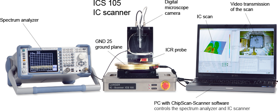
Figure 1 shows an IC test set-up for measurements based on the surface scan method according to IEC 61967-3. Today we can say that three types of microprobes are necessary to detect the whole electromagnetic field in the μm range. For this Langer EMV developed several microprobes, each probe determined for a special case:
- E-field probes are built to detect the electric field.
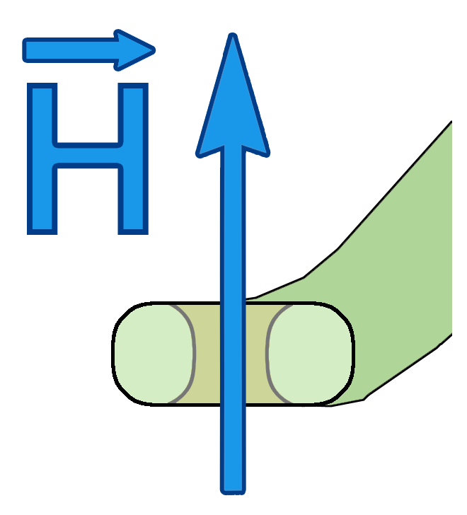
- H-field probes are considered to measure the magnetic field. For this purpose two magnetic field probe types are required to measure magnetic field in all directions: The “H” type H-field probe is sensitive for vertical magnetic field and the “V” type H-field probe for horizontal magnetic field. The directional characteristic of the “V” H-field probe has two zero values for physical reasons. The field components located in the plane of the vertical probe can only be detected by rotating the “V” H-field probe.
The IC scanner brings the microprobes in position providing a high mechanical resolution and high repeatability. For measuring an electromagnetic field with high resolution the accuracy should be at least 20 µm and the repeatability smaller than 5 µm. At least four axes are necessary to completely detect EMC emissions from ICs. Three axes are required for the movement in X-, Y- and Z-direction and a fourth is to rotate the microprobe - necessary for vertical H-field probe.
The basic design of the microprobes is constructed to match with the Langer EMV IC scanners. Furthermore the mounting option of the microprobes was expanded to fit also to common scanner systems.
The third part of the measuring system is a PC with a control and measurement software. Functions are: detection of all connected devices, control of the IC scanner system, initialization of the spectrum analyzer, getting the measuring results from the spectrum analyzer and visualization of the measuring results in a descriptive way. EMC emission measurements on ICs provide large quantities of data which are compiled in six dimensions in a database.
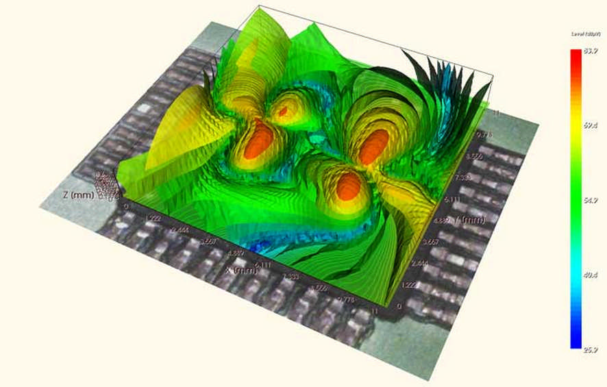
Not all six dimensions can be represented graphically at the same time, thus the representation is reduced to feasible five dimensions. Figure 2 shows an example for a volume scan over an IC with a vertical H-field probe at a specific frequency.
3 Near-field Microprobes
3.1 Probe design
The IEC 61697-3 describes the parameters of microprobes, for example the mechanical construction, frequency range and resolution. According to the IEC standard, the probe tip has to consist of a semi-rigid cable with a single coil for measuring electromagnetic emissions. The disadvantage of this measuring setup is, it could not differentiate how much of the measured voltage at the probe tip is a result of magnetic or electric coupling effects. Because of this Langer EMV designed two different types of microprobes, one type for measuring the electric field and one for measuring the magnetic field. The magnetic field microprobes are additionally shielded against coupling of the electric field. The microprobes therefore allow the user to separately examine electric and magnetic emissions on ICs and DIE surfaces, e. g. bonding wires and pins. It is also possible to measure with a magnetic probe above a conductor or IC pin and thus make a conclusion about the current which is floating through the conductor.
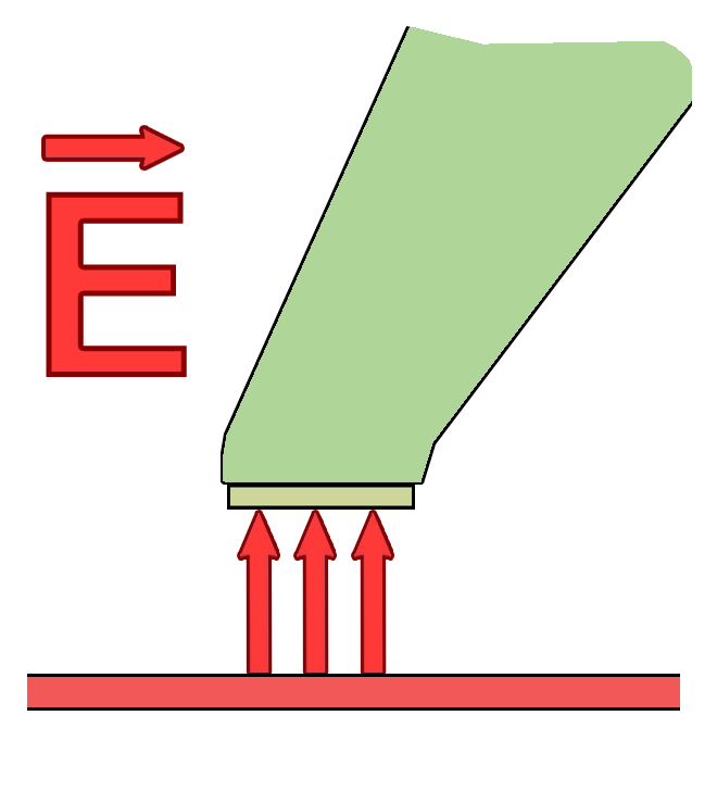
Currently with an E-field microprobe a resolution down to 65 μis possible. Figure 3 a) shows the general construction of an E-field microprobe with a sensitive electrode (light green) and the shield (dark green).
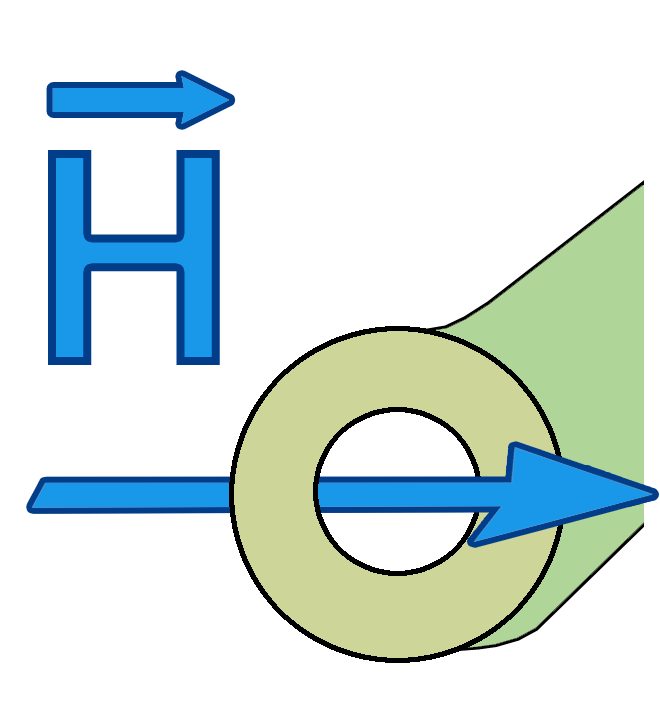
The resolution of the H-field probes is defined by their inside diameter. The magnetic probe tips consist of a coil with specified winding and inside diameter, refer to Figure 3 b) and c). Both these parameters basically define the size of magnetic field (resolution) and the magnetic field strength which is detected. Today the smallest inside diameter is specified at 100 μm, for horizontal and vertical polarization. This results in a resolution of the measured magnetic field down to 80 μm.
All magnetic probes are shielded against the electrical field. The quality of the shielding will be discussed in chapter 4.
All microprobes are equipped with an internal pre-amplifier. The amplifier allows to detect also low signals clearly. The frequency range of the microprobes is defined at 1.5 MHz up to 6 GHz. The range will be extended to a higher frequency, so it will go along with the IC development to higher clock cycles.
3.2 Magnetic field strength and current determination
Magnetic field strength correction:
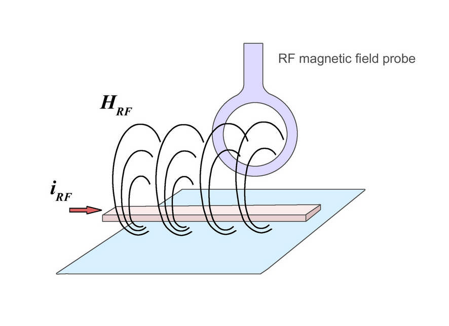
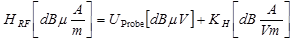
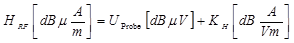
The magnetic field strength HRF in the magnetic field probe coil can be calculated from the voltage output signal UProbe of the magnetic field probe by means of the correction characteristic. The correction factor KH of the magnetic field microprobe is independent of the measurement geometry in each individual application, i.e. the probe can be guided at an arbitrary distance and angle relative to the electric conductor without any correction error (Figure 4). The result is the average magnetic field that is enclosed by the probe coil.
Current correction:
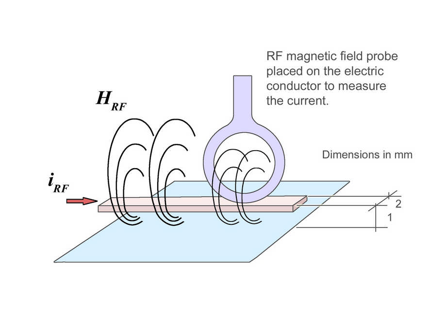
There is a consistent physical correlation between the magnetic field HRF and the current IRF which depends on the geometry of the current conductor layout. The given correction factor KI thus refers to a defined reference set-up.
The determined current values ICorr are only correct if the geometric parameters coincide with the reference set-up (Figure 5) when the probes are used. If there are deviations from this set-up, the current values ICorr will also deviate. So the calculated current value ICorr can only be used as an orientation value.
Use of the correction factor KI in the adapted quantity equation:
4 Measuring above a Stripline
Due to its design, each microprobe type has a special measuring characteristic. In the following test cases we will discuss both H-field probe types - the horizontal and the vertical:
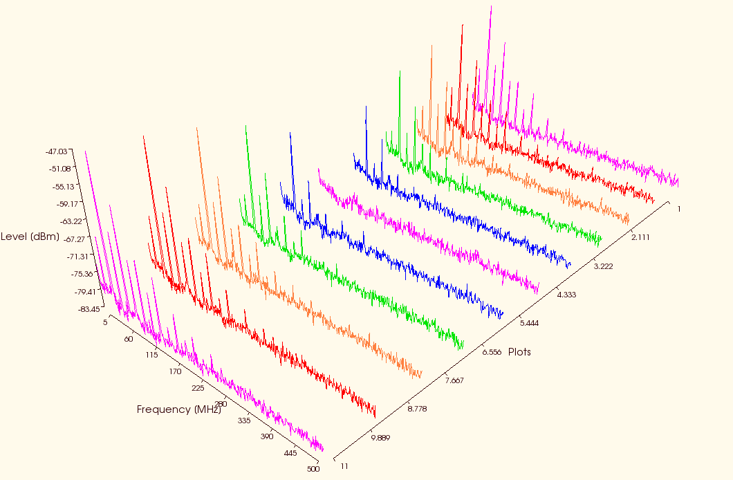
The measurement is based on the following parameters: The stripline has a width of 25 μm, distance to ground 20 μm and termination of 50 Ω. The low end of the probe tip is adjusted to 20 μm above the stripline. The stripline is powered by the tracking generator of the spectrum analyzer with a voltage level of 100 dBµV. The microprobe was moving above the stripline on a straight line, length 3 mm and measuring steps 30 μm. Figure 6 and Figure 7 show the measuring result for both H-field types. For each measuring point (plot) the amplitude in reference to the frequency is indicated.
As indicated above, both probe types are measuring in a different way. The horizontal probe measures a minimum at the centre of the stripline. Intensive magnetic fields are located at the edges of the stripline, which is also the site of the respective local maximum values of the scan volume. This behaviour depends on the direction of the magnetic field lines and on the position of the measuring coil in relation to the field lines. At positions where the coil is parallel to the field lines, the probe could not detect a magnetic field.
Unlike the horizontal polarized probe, the vertical probe measures high magnetic field strength over the conductor path. At the edges of the stripline the vertical version measures a local minimum.
In each test case the amplitude and the width of a measured minimum or maximum depend on the distance of the probe tip to the measuring object and the width of a measured stripline or any other electrical line.
5 IC Scan
5.1 IC Volume Scan
In the following test case two surface scans were done at IC level. The DUT was a 8051 model, system clock at 20 MHz,
The first scan was done with a horizontal H-field probe and the second with a vertical one. The following settings were met:
- Scan Volume: 11.0 x 11.0 mm
- Step width: 200 Ωm
- Points in the volume: 10.000
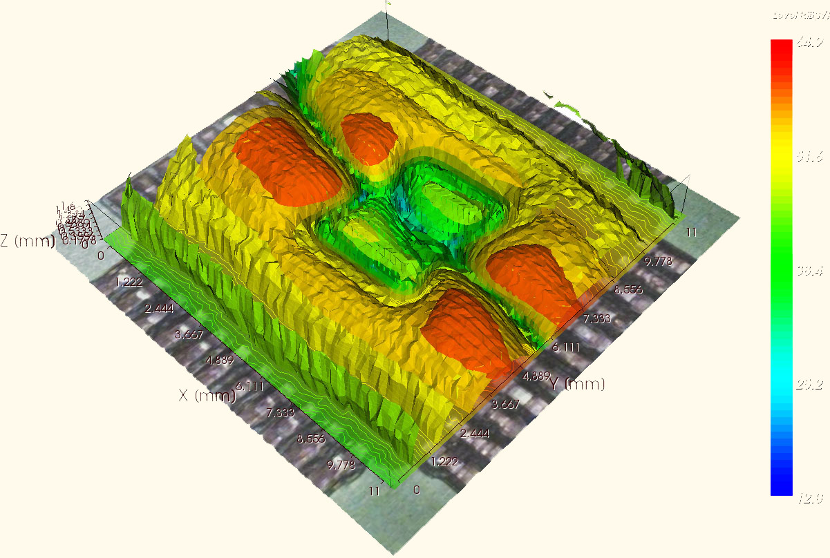
The driving of the scanner, the detection and the interpretation of the measuring results were done by ChipScan-Scanner software. Figure 8 shows the measurement set-up. As it is shown, the IC was mounted on a ground plane. All other electrical parts were mounted on the back of the ground plane. This set-up helps to minimize side effects from other electrical parts. Three pins were used for driving LEDs to monitor the program. All other pins were programmed as inputs.
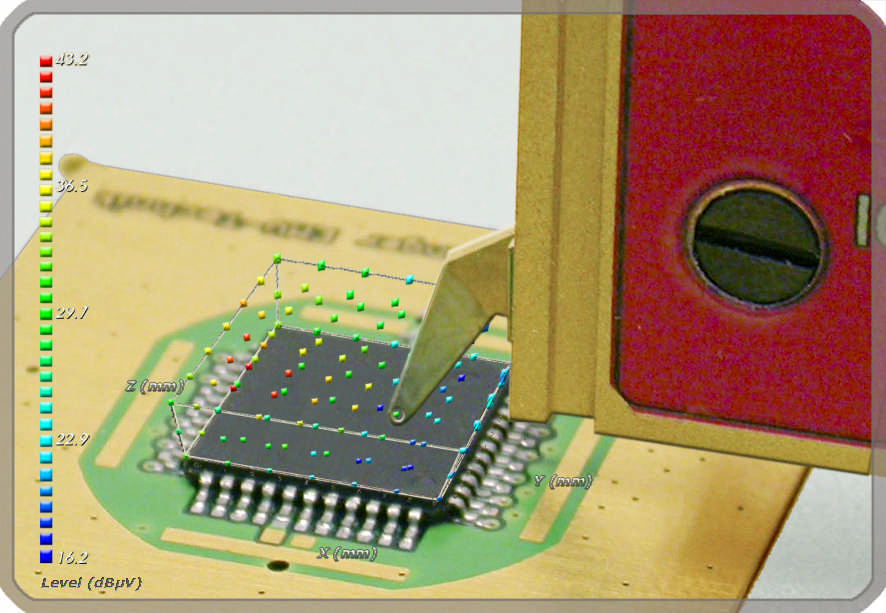
The measurement results are shown in Figure 9 and Figure 10. The bar on the right side of both screenshots shows the relation between color and strength of the magnetic field. Red means a high signal strength of approx. 80 dBΩV and blue stands for 20 dBΩV.
Both measurements were done above the same DUT, but with different equipment. As discussed in chapter 4, the horizontal H-field probe measures a local minimum directly above the current run, and on the edges a local maximum. These can also be seen in Figure 10. From the Vcc pin the supply current flows via the bond conductor into the IC. At the chip the current takes different paths and returns via the bond conductor and the Vss pin to the board.
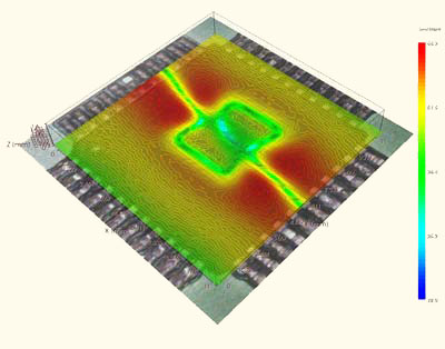
The vertical H-field probe could only measure the magnetic field, where the current flows parallel to the measuring coil. So there are some parts where the magnetic field is measured, especially in the power supply region of the IC. In other parts of the IC the microprobe is hardly detecting any magnetic field. This could be because there is no magnetic field or the magnetic field is not in the sensitive probe direction.
As a consequence of this, a second measuring should be done, where the measuring coil (microprobe) is turned by an angle of 90°. This way the magnetic field could be detected, which stands 90° to the firstly measured one.
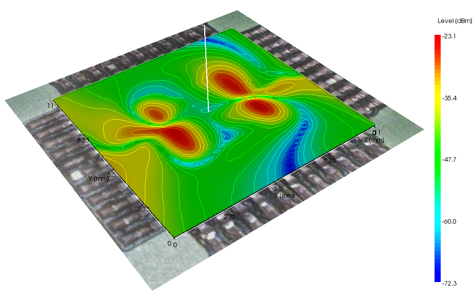
If such a surface scan is done in different distances to the IC the magnetic field can be displayed in the entire volume above the IC. In Figure 11 all points with the same field strength are connected.
This diagram serves as a source for further learning or understanding about coupling effects from the IC to other metallic parts which could be placed near to the IC in real applications – e.g. a heat sink, connectors, shielding parts.
5.2 IC-Pin Scan
Using a vertical H-field probe offers the additional possibility to measure high frequency current flowing through IC pins. Following the basic measurement set-up like in Figure 4 it is very simple to automatically place the probe close to every IC pin and measure the current. One result is shown in Figure 12.
Typically, each pin of an IC can be a source of high frequency current – power pins and output pins as well as input pins. It depends on the IC itself and the impedance of the connected electronic circuit. So the knowledge of these currents enables the designer of the board an opportunity to place series resistors or capacitors to GND in an optimal way.
6 Conclusion
In this paper a measurement method to detect a magnetic and electric field in the µm range is introduced. It is shown that the measuring of near field above ICs or open DIEs with microprobes is a perfect tool for engineers, to detect EMC issues and to solve these in a reliable way. The measuring could be done on reference PCB assemblies or on the PCBs of the customer.
In the future there will be a lots of opportunities to improve the measurement of electromagnetic field in the µm range. With a smaller resolution the detection over DIEs could be done more precisely, so also smaller parts of integrated circuits could be scanned with a higher resolution. The frequency range has to also be widened. Because of higher clock frequencies the product norms will be adjusted, so that there will be additional requirements for EMC disturbance in the higher frequency range above 6 GHz.