

From Device testing to the IC-Test System Part 1
Introduction
Compliance with EMC requirements is becoming increasingly demanding. While technical progression has allowed for reductions in feature size, this has also lead to the particular challenge of controlling a device’s immunity.
These increased requirements regarding immunity add substantial costs to the development and manufacture of devices. By testing immunity at a component level (i.e. ASICs and ICs), however, countermeasures can be more easily identified and taken. These immunity test results allow for specific ICs and ASICs to be preselected for further module development. Additionally, they can be incorporated into IC and ASIC development and contribute to component optimization.
Although there are already testing procedures in the industry that have provided a wealth of experience in evaluating IC and ASIC immunity, the concept behind the current testing method is such that interference pulses are applied directly to the pins of the test ICs. The shape and amplitude of the applied interference are specifically selected to mimic the typical interference to which the IC would be subjected when the device into which it will be placed undergoes a standardized immunity test or is in a disturbed environment.
During operation, technical equipment, facilities, and devices are generally supplied by pulsing interference signals. Accordingly, the standard device tests simulate, for example, the spark generation at a switch contact (burst) or electrostatic discharge (ESD).
With the standard testing method, immunity in active mode (i.e. the behavior of the functioning voltage-supplied ICs) is observed. The criterion for passing the test is undisturbed function.
Environmental influences or the test itself can cause voltages and currents that are significantly higher than the specified maximum values for ICs.
Analyzing immunity at the IC-level, however, has the benefit of not requiring the consideration of impact of the device’s design on EMC. This includes, for example, the design of the printed circuit board, the nature and availability of the connector, or the housing construction.
Moreover, when testing IC immunity, interference effects are less pronounced than when testing the [entire] device. This results in a better reproducibility of the test results.This document describes the connection between the device test and the pin granular IC test.
Device testing
Because of the constant increase in digitization and widespread use of electronic products, which requires a high degree of robustness regarding device immunity, it is particularly important to conduct immunity tests with pulse-shaped interferences when testing technical facilities and devices. This is because they will also be subjected to the pulse-shaped interferences in operation and during standard use.
The relevant interference pulses (burst and ESD) of the immunity tests are described in the following standards: IEC 61000-4-4 fast transient immunity test (burst) and IEC 61000-4-2 electrostatic discharge immunity (ESD):
| IEC 61000-4-4 | fast transient immunity test (burst) |
|---|---|
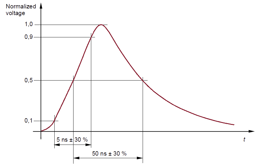 | |
| Figure 1 Time curve of a burst pulse according to IEC 61000-4-4 | |
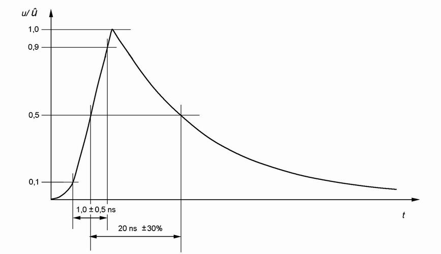
With a source impedance of 50 ohms pulses from a minimum of ±2kV with a leading edge of 5 ns and a trailing edge of 50 ns (half amplitude) are applied to the device (Figure 1). It is from these pulses that bursts are comprised.
| IEC 61000-4-2 | electrostatic discharge immunity test (ESD) |
|---|---|
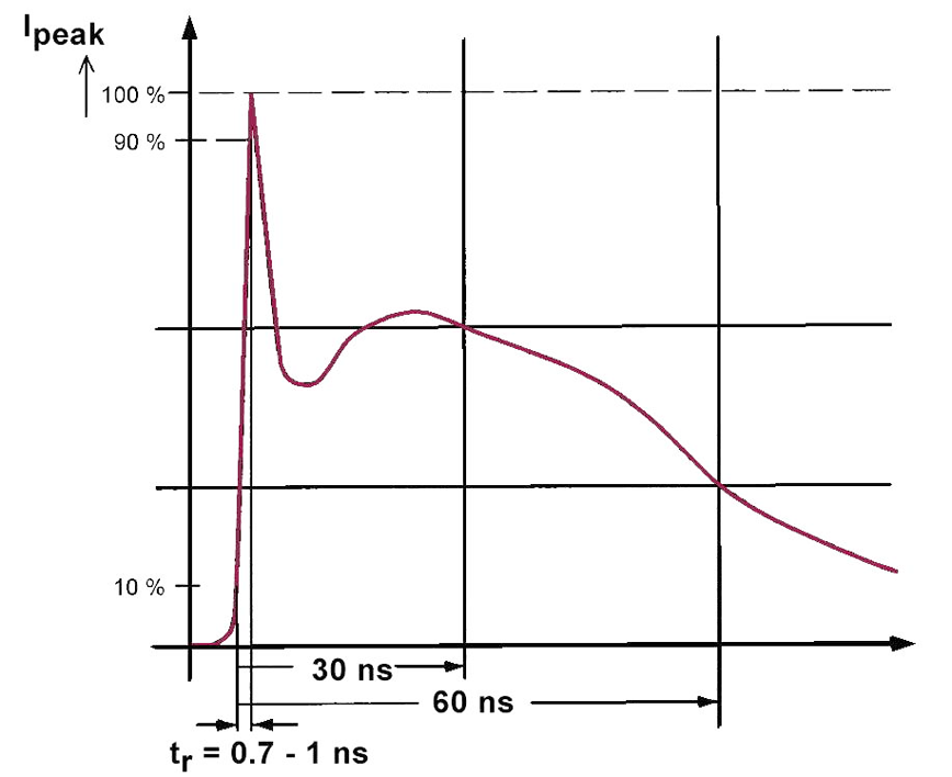 | |
| Figure 2 Time curve of an ESD pulse according to IEC 61000-4-2 | |
With a source impedance of 330 ohms pulses of at least ±6 kV with a leading edge of 0.7 ns and a trailing edge of 5 ns (half amplitude) are applied to the device (Figure 2)
Basic Principles of Interference Regarding Device Testing
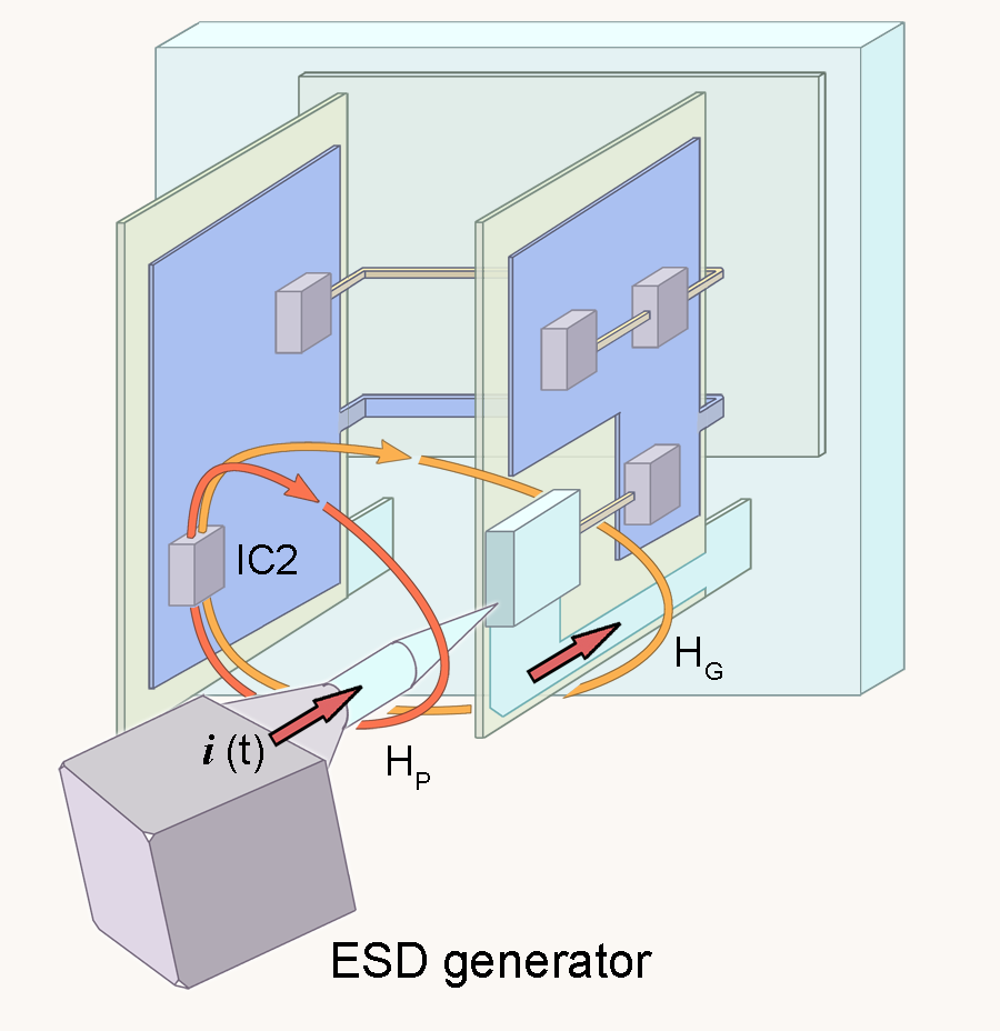
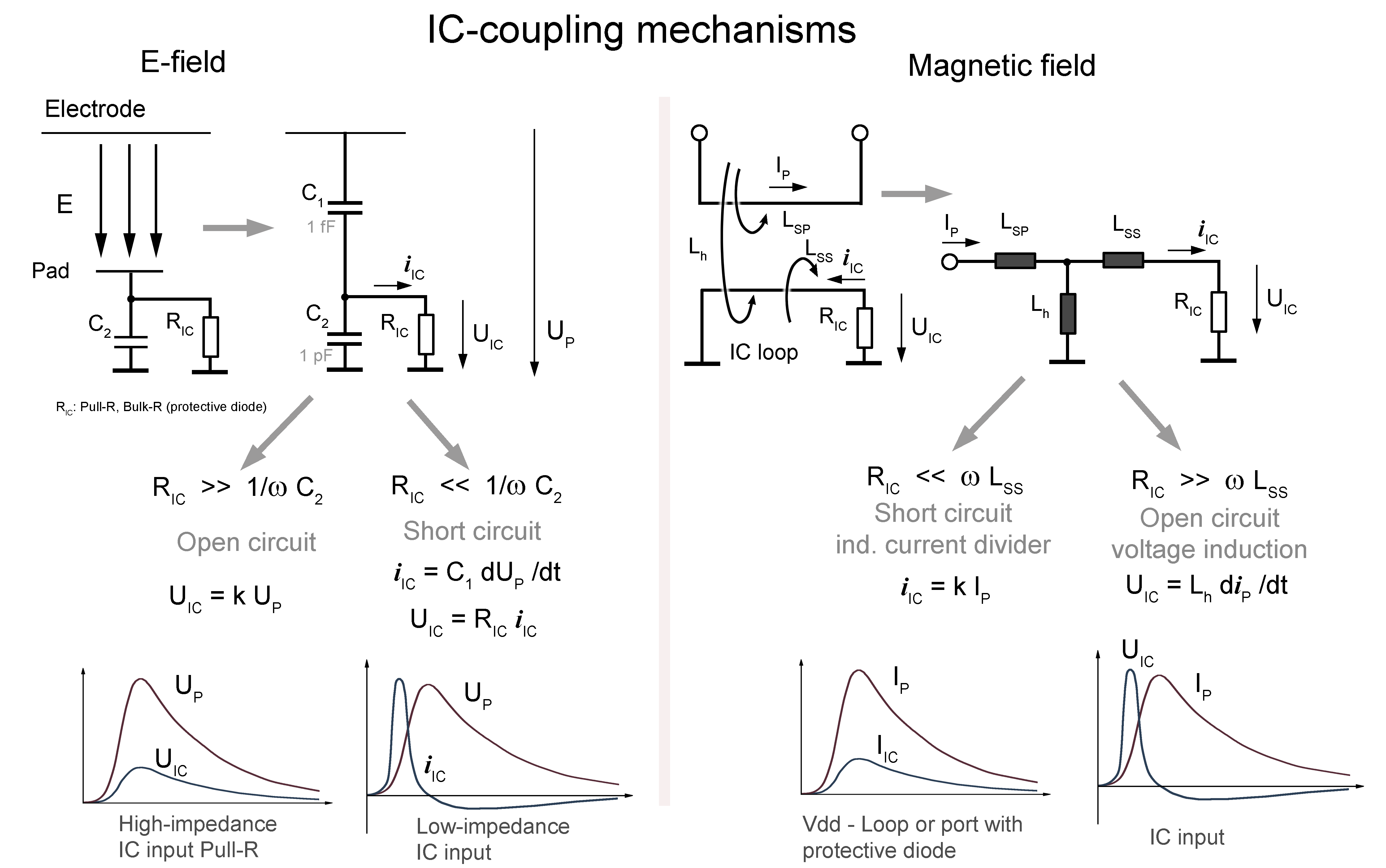
In order to demonstrate its immunity, a pulse-shaped interference is applied to the device both in and independent of its intended location. A primary disturbance pulse (ESD or burst) of the voltage u(t) applied to the device causes a pulsing interference current i(t) to flow through the device (Figure 3). Two fundamental mechanisms – magnetic coupling and electric field (E-field) coupling – though simultaneously occurring, should be individually considered.
1. Magnetic Field (Inductive) Coupling
Magnetic-field interference H(t) forms around the conductor carrying the interference current i(t). The lower the impedance of the primary circuit, the higher the current flow and, thus, the higher the H-field will be.
In the ideal case, the field strength of a straight conductor is given by:
| [1] | 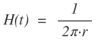 |
The magnetic-field interference penetrates the device and the surrounding components and printed circuit boards. Conductor loops are located on the printed circuit boards or in the components (e.g.: IC, Figure 3). The magnetic-field interference induces a secondary interference voltage u_sec(t) through the inductor L.
| [2] | 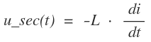 |
This interference voltage could exist, for example, on an IC pic or in an IC, which may cause the IC to malfunction.
2. E-field Coupling
The primary disturbance pulse (ESD or burst) of the voltage u(t) applied to the device causes a voltage drop across the assembly (Figure 4). The electric field E(t) is obtained from the voltage difference along the observed geometry. The higher the impedance of the primary current path, the higher the voltage difference and, thus, the higher the resulting E-field will be. The E-field transfers the interference as a displacement current i(t) in secondary loops such as [at] signal cables and/or IC pins via capacitive coupling. This process can be achieved by a coupling capacitance C which is in the fF range, as described in [3] below. An interference voltage is created at the internal resistance of the secondary loop by the capacitive-coupled current i(t). This interference voltage may be present at an IC pin and trigger interference in the IC.
| [3] | 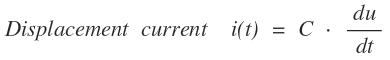 |
In both cases (coupling caused by a magnetic- or E-field) the disturbance is reduced by a factor of one (the device factor) during the transition from the primary disturbance circuit to the secondary loop and is located on the active electronic (eg, on the IC). The 6kV interference voltages that usually occur during an ESD device test decrease to a range of ...0.1 V to several 100V. This decrease is dependent on the impedance in the primary and secondary disturbance circuit.
ICs mounted on the printed circuit board are exposed to disturbance-driven magnetic fields H(t) and E-fields E(t).
Magnetic-Field (Inductive) Coupling into ICs
The magnetic flux density Bst(t) penetrates the smallest conductor loops (eg, between an IC and an attached decoupling capacitor, Figure 5). A voltage Ust is induced in the circuit loop by the magnetic flux Φ, as described in [4] and [5].
| [4] | 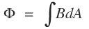 |
| [5] | 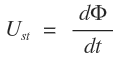 |
The voltage Ust drives interference current into the IC. The impedance of this interference source is low due to the formation in the conductor loop. This can lead to high currents Ist(t).
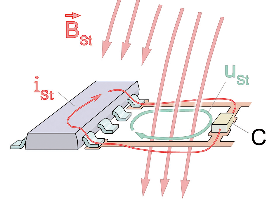
E-Field (Capacitive) Coupling into ICs
The electrical field strength E(t) or the conductive-surface-related displacement current D(t) generates interference Ist(t) in the conductor (Figure 6). This interference causes a voltage boost Ust(t) on the conductive surface. This voltage boost can distort logical signals, which are transmitted over traces. The displacement current Ist(t) can also be incorporated into ICs and trigger further disturbance events. The “electric field” interference source has a high impedance.
Simulation
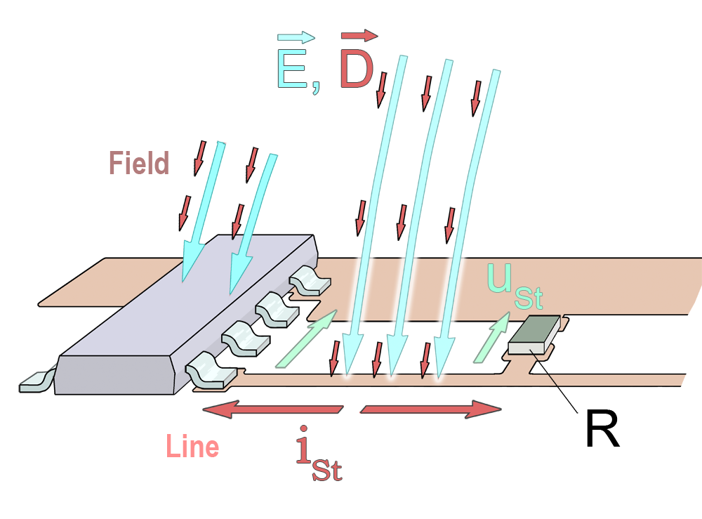
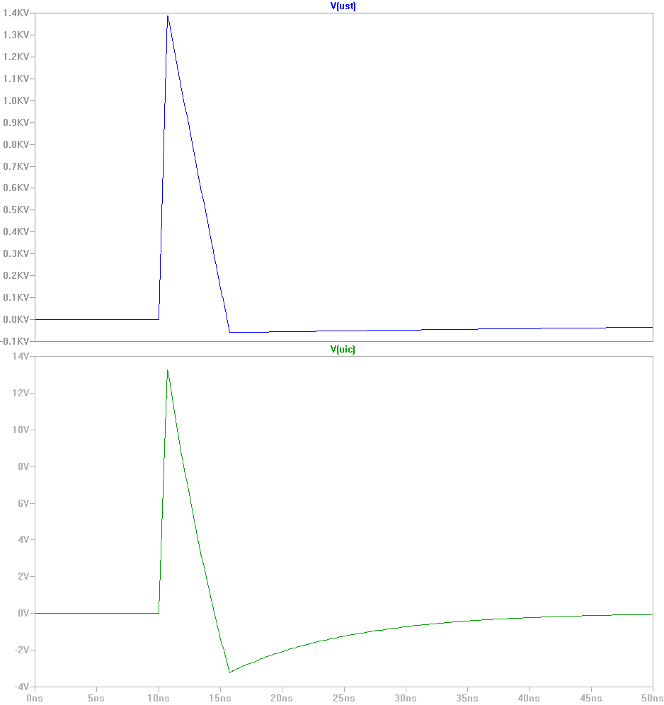
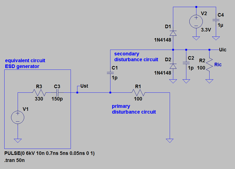
The following simulations (Figures 7-12) demonstrate the general conditions. In Figure 7 the generation of the ESD pulse has been greatly simplified. The equivalent circuit is based on the principles of capacitive coupling seen in Figure 4.
Estimating the interference voltage at the IC
A positive interference pulse with amplitude of 6kV is injected as a contact discharge in the primary disturbance circuit (Figure 7). An interference voltage peaks (Ust) of 1.4 kV originate at the primary impedance R1 (Figure 4). The 13.5 V interference voltage remains in contact with a high-impedance IC pin through capacitive coupling (E-field coupling) across C1. The impedance of the primary disturbance circuit can be significantly larger (1kOhm), so that the interference voltages at the IC pin can exceed 100V. This allows for the Maximum Ratings specifications of ICs to be significantly exceeded.
Coupling Modes
The type of coupling is also dependent on the ratio of the source impedance to the load impedance, i.e. to the input impedance of the IC.
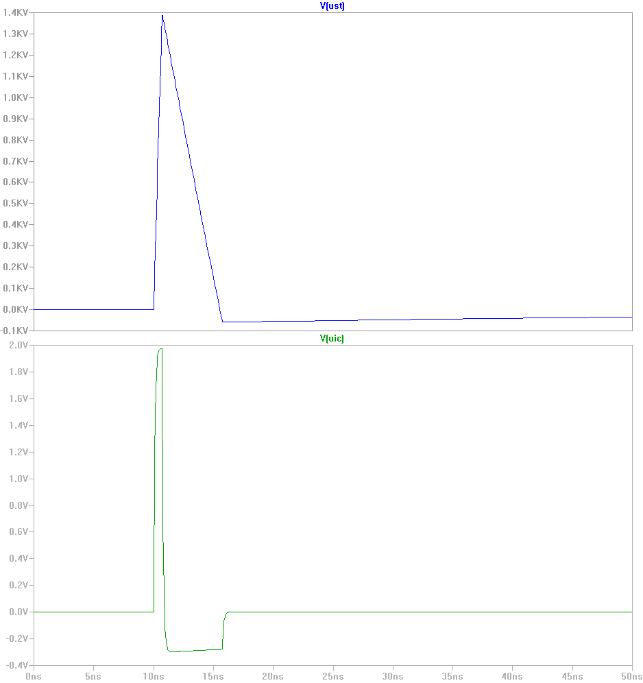
E-Field (Capacitive) Coupling
With a slope of 1 ns resulting in a transfer maximum rate of 1 GHz. A coupling capacitance C1 of 1 pF is assumed. The coupling capacitance then has an impedance X of 159 ohms. When the IC’s input resistance is 10 k, the input resistance is much greater than the source resistance (impedance of C1). Consequently, the adjacent interference pulse at R2 (at the IC) has the same waveform as the primary interference pulse. This results in a proportional voltage division with the capacitive divider C1, C2.
Ri of the IC ≫ XC1
Completely different conditions are obtained when the load impedance is smaller than the source impedance. The following example assumes R2 = 100, C1 = 10fF.
Ri of the IC < XC1
Under these conditions, the primary interference pulse is differentiated at the IC (Figures 9 and 10).

H-Field (Magnetic) Coupling
With H-field coupling, the conditions are reversed. In the idle state
Ric ≫ Xss is differentiated,
Ric < Xss is current divided.
The summary of coupling mechanisms is shown in Figure 11. In H-field coupling the transformer equivalent circuit diagram with the main inductance (Lh) and leakage inductance (Ls) is assumed.
Literature of Part 1:
| /1/ | "Richtlinie EMV-Anforderungen und Prüfverfahren zum Test der Pulsstörfestigkeit von ICs und ASICs" Langer EMV-Technik GmbH |
From Device Testing to the IC Test System Part 2
IC Effects
Protective mechanisms have been integrated into ICs in order to prevent the destruction of their sensitive structures caused by surges.
Because of the way these existing protection systems are designed, it is assumed that the IC to be protected is not powered by a supply voltage, i.e. it is not in operation.Thus, the IC is protected against high electrostatic voltages, which are likely to occur during the manufacturing, transporting, and processing of electronic devices.
In contrast to the design of existing IC protection systems, the IC in the previously described device tests is powered by supply voltage and, thus, is in operation.
Under interference during practical operation (IC power-supplied), protection circuits can inadvertently cause internal shorts.
The protective mechanisms integrated into the ICs are generally not made public by the manufacturer. However, one can assume the following mechanisms:
- Electrical surges at supply connections are limited by structures which functionally correspond with Z-diodes.
- Overvoltages at inputs and outputs are limited by diode- or transistor structures.
The load impedances are dependent on the IC pin to be tested. Power supply connections can be characterized by low load impedance. At these connections a capacitively coupled signal is differentiated as described above. If the signal is inductively coupled, the voltage will split. When maintaining the specified level range of the protective circuit´s limiting voltage, the impedance at IC inputs will be relatively high. If this range is exceeded, the capacitively bridged supply system will cause a drastic reduction of the impedance at the protection circuits and power supply.
This results in a combination of voltage-dividing behavior and differentiation of the voltage limiting effect of the protection elements. When the interference current flows into the IC through the protection circuits, internal function errors can be triggered.
Depending on the characteristics of the diodes, different curve traces occur. Slow Si diodes were used in Figures 1 and 2.
The significant interference current I(D1) which flows into the power supply system via the diode, is apparent. This can be seen in Figure 2. It is important to consider that this situation occurs not only during the device test (according to IEC 61000-4-2), but also during the normal application of an IC when electrostatic discharge occurs.
Required Pulse Width for the IC Test
The objective of defining a test pulse for the immunity testing of ICs is to be able to reproducibly test ICs with a broad spectrum of structural widths. This is because the internal processing speed of an IC is dependent on its structural width. A coarse structure IC, for example, will have some inertia against disturbance events.
The dynamic switching threshold/disturbance threshold can be used as a basis for evaluating ICs.
Figure 3 shows the pulse width T of the disturbance pulse on the X axis and the disturbance threshold on the Y axis. For wide pulses (Figure 3, > 1.5 ns), the disturbance threshold is near constant (static disturbance threshold). For short pulses (Figure 3, < 1.5 ns), the disturbance threshold increases and the IC becomes insensitive (dynamic disturbance threshold). The boundary of the static/dynamic transition is dependent on the IC’s structure width.
In the case of disturbances via power supply systems, additional behavior patterns should be considered. As determined in Figure 3, the pulse width of the test generators used to test the IC must be > 1.5 ns. Due to the push for better and faster technology, this limit is fluid, allowing for faster ICs with pulse widths of < 1.5 ns.
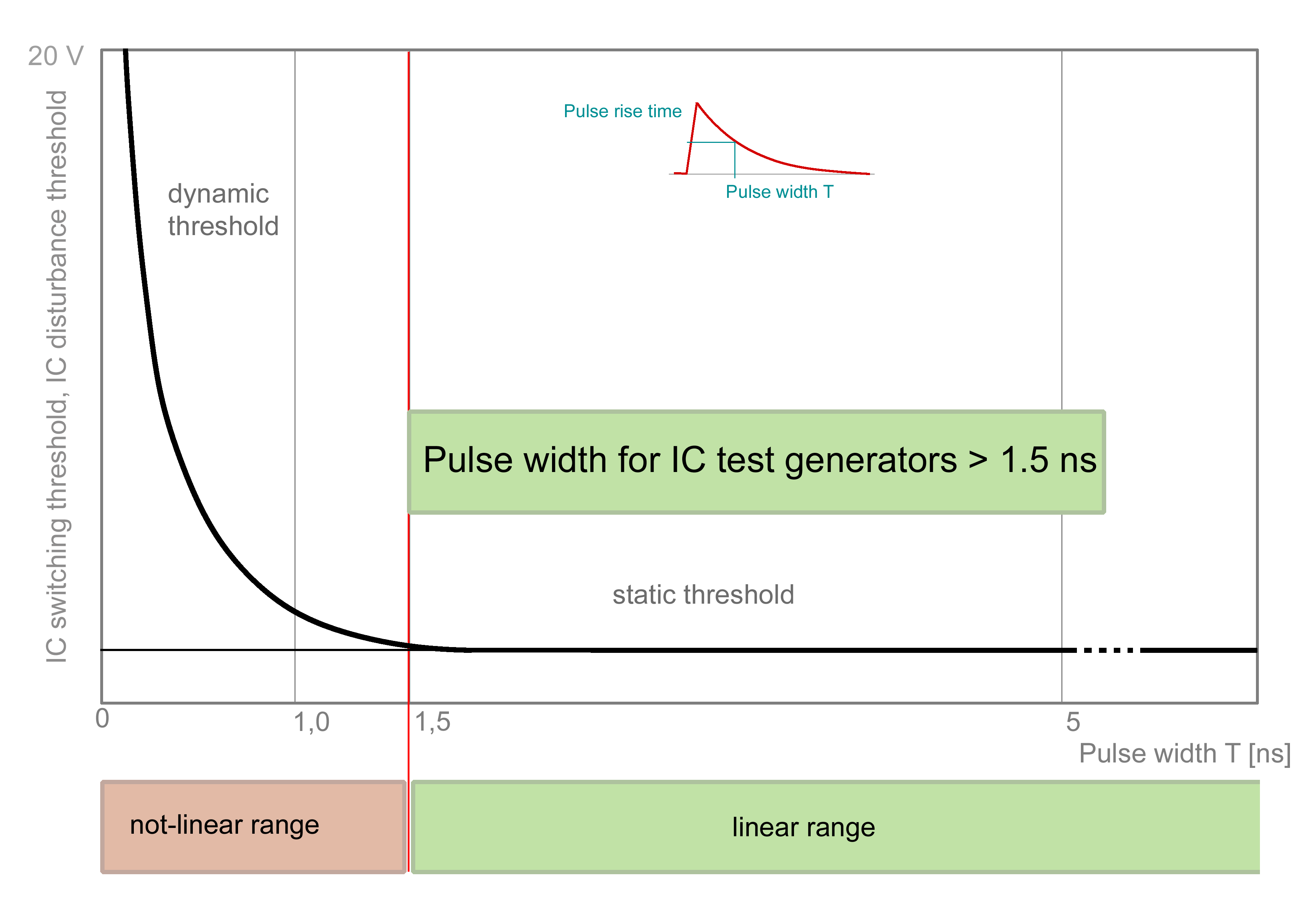
For reproducible results it is necessary to select a pulse width for IC tests within the linear range, i.e. in the range of the static disturbance interference threshold.
20 years ago an IC with a disturbance pulse of 2 ns was not able to be disturbed. As technology advances, structure widths decrease and the transition from static to dynamic ranges shifts toward shorter pulse widths.
Consequently, today’s test pulses in the static range can also be used for ICs of faster and future technologies.
Conversely, however, it must be noted that ICs with smaller structures and lower supply voltages have lower disturbance thresholds and an increased sensitivity. Thus the importance of immunity tests will only increase in the future.
The IC Test Method
According to preliminary considerations, pulse sources with low and high impedances should be available. The following should be considered: replacement circuits, edge steepness, and the maximum voltage levels.
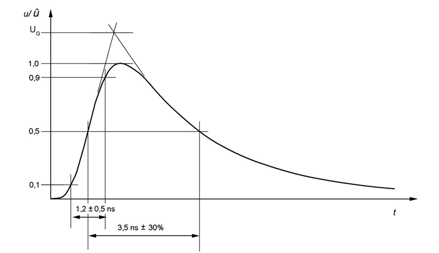
The pulse source with low impedance (Probe P2xx) is intended to test power supply connections. For this purpose the support capacitor is removed from the circuit to be tested. It is replaced by the CP capacitor, which is located in the probe. The pulse width of Probe P2xx is formed from the leading and trailing edges and is 1.2 ns/3.5 ns in the range of the static disturbance threshold.
Pulse Source with Low Impedance (Low-Impedance Probe P2xx)
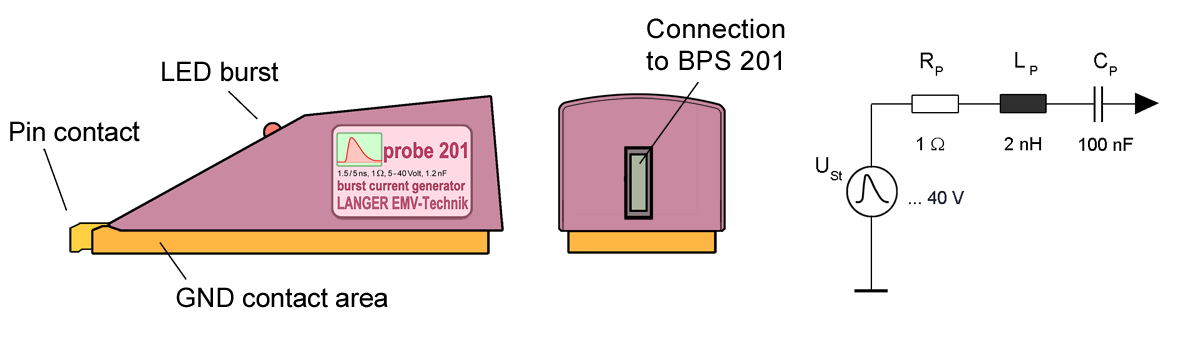
| RP = 1 Ohm |
| LP ≤ 2 nH |
| CP ≥ 100 nF |
| Voltage up to approx. ± 40 V |
Pulse Source with High Impedance (High-Impedance Probe P3xx)
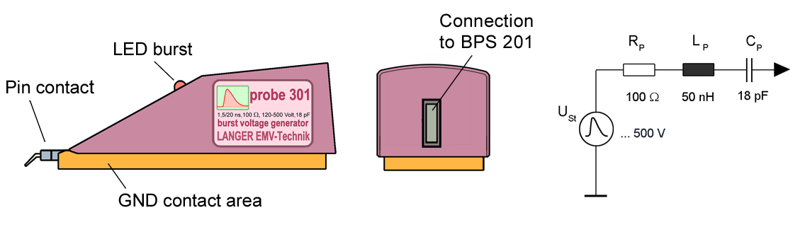
| RP = 100 Ohm |
| LP ≤ 50 nH |
| CP = 18 pF |
| Voltage up to approx. ± 500 V |
The pulse width of Probe 3xx is formed by the leading and trailing edges and is 1 ns/20 ns within the range of the static disturbance threshold. In case of a short circuit, the pulse width of Probe P3xx decreases to 2 ns. This occurs when the protective circuitry becomes conductive to reestablish the pulse width in the range of the static disturbance threshold. The disturbance pulse is further widened by internal transient processes.
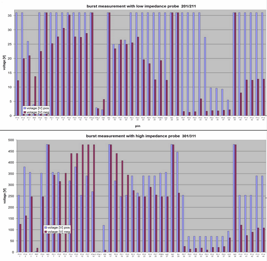
Figure 8 shows the pin disturbance threshold of an IC on a granular level.
With some comparative experience, it is possible to identify particularly vulnerable pins. Exposed pins should withstand > ±15 V disturbance threshold of the low-impedance source and > ±150 V of the high-impedance source.
Simulation with IC Test Pulses
To assess the effects of the described test pulses, the test pulse simulation models can be used.
This helps the manufacturers of ICs or ASICs to predict the results of the proposed test method. Notable is what occurs inside the ICs during interference; which circuits are affected and how. Internal parasitic elements, such as line inductances and parasitic capacitances, as well as the actual protective structures, of which only the manufacturer of the IC is aware of, play an essential role.
Disturbances in the internal supply system, in addition to signal distortion, play a decisive role in fault analysis. External signal distortion can generally be controlled by design measures such as telegram repetitions, error correction, etc. They cannot be controlled, however, if the disturbance event results in the collapse or oscillation of a part of the internal supply. This affects the overall function of the IC.
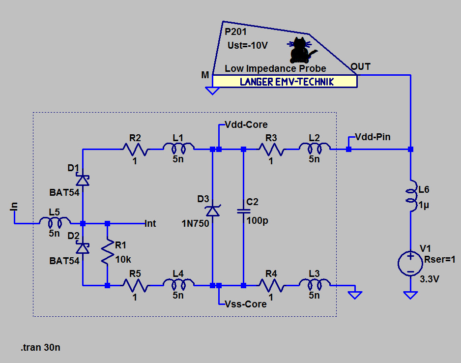
In Figure 9 the LTSpice model of the high-impedance Probe P301 is connected to the input of a simplified IC equivalent circuit. The input consists of protective diodes D1 and D2, which are connected to the Vdd and Vss system of the IC. The equivalent capacitance C2 (100pF) represents the core of the IC. The most important circuit elements are actualized by L1-L4, R1-R5, and D1-D3. The power clamp D3 protects the core from surges.
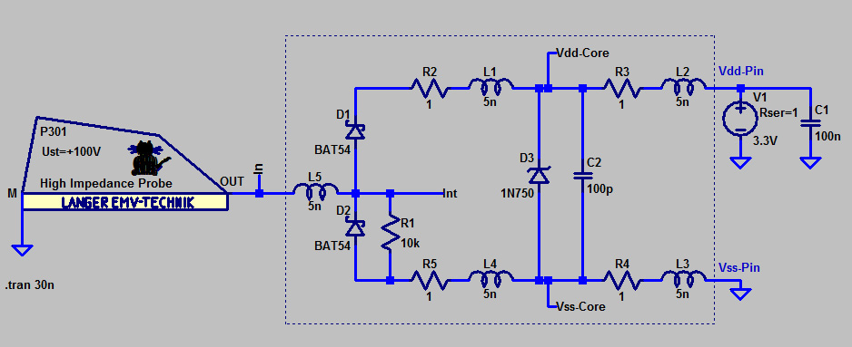
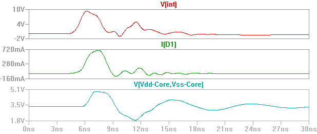
For a test voltage of +100 V, the disturbance voltage V(int) is produced in the IC. The current I(D1) flows through the protective diode D1. The current reloads the core capacity. In the interior of the IC, a transient response occurs on the supply system V(Vdd-Core, Vss-Core) (Figure 10). In this case, the core’s voltage drops from 3.3 V to 1.8 V and can lead to a failure of the IC.
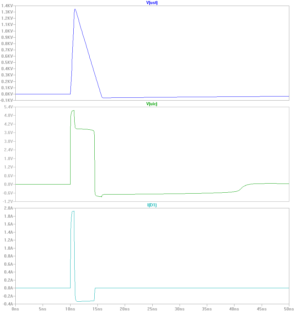
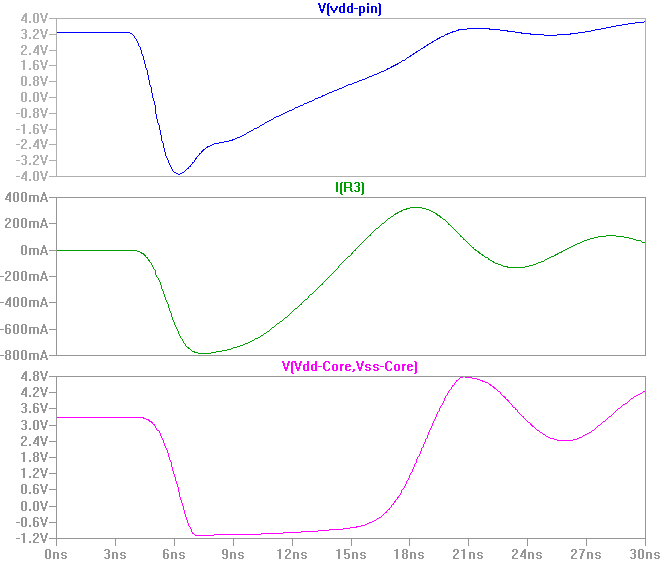
In Figure 11, the LTSpice model of the low-impedance Probe P201 is connected to the Vdd pin of the IC equivalent circuit. The backup capacitor C1 has been removed and replaced by the Probe P210. A voltage of -10 V has been set in the Probe P201. The disturbance produces a voltage drop to -4 V at the Vdd pin (Figure 12). The disturbance current flows mainly through the power clamp D3 and the core capacitance C2 to the Vss. As this occurs, the core’s voltage V(Vdd-Core, Vss-Core) drops down to -1.2 V. This certainly interferes with the function of the IC.
The phenomena shown in Figures 11 and 12 only illustrate the processes of ICs exemplarily. Thus a problem-solving approach to understanding highly complex disturbances in ICs is demonstrated.
By combining the LTSpice simulation and tests with real ICs and probes (P201 and P301), efficient development tools are available to investigate and improve the EMC characteristics of ICs. The LTSpice models of the test generators make the described test procedures more accessible to IC manufacturers. In the future, one should be able to specify EMC properties at the beginning of an ICs development.
Literature of Part 2:
| /1/ | LTSpice-Simulationsmodelle für IC-Testpulse P201 / P301: https://langer-emv.com/de/category/simulation/76 |