

New developments in electronics manufacturing are increasingly dominated by the requirements of EMC today. Considerable follow-up costs in product development are caused due to the failure of electronic modules in EMC compliance tests. The integrated circuits that are used in an electronic system are decisive for its EMC performance as a whole. ICs are often responsible for interference emissions or immunity weak points and it is difficult to gain control of them in such cases.
The structures of ICs have become smaller and smaller over time which has led to higher switching rates and made a reduction in the supply voltage necessary. Due to these two factors, ICs have become more susceptible to ESD.
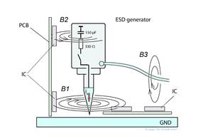
In EMC compliance tests according to the standard IEC 64000-4-2, electronic devices are tested with an ESD generator (ESD gun). The ESD generator produces a current pulse (Figure 3) as required by the standard, which is injected into the device under test (Figure 1). This ESD pulse is coupled into metallic parts of the electronic device and, from there, moves to the IC via conductive and capacitive/inductive coupling. The amplitude of the disturbance pulse is varied with time on its path to the IC. The objective of this report is to investigate the coupling paths to the IC. The amplitude of the disturbance pulses that affect the IC is measured as a function of time for the individual coupling paths. This helps identify which coupling is relevant and which parameters (rise time, voltage intensity, waveform, amplitude, current, voltage, electric or magnetic field) have an influence on coupling. These findings allow the development of selected EMC countermeasures to protect the IC.
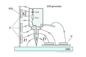
Apart from the current pulse according to the standard, the ESD generator induces a magnetic and an electric field (Figure 1, Figure 2). Due to the discharge current, a magnetic vortex field is produced at the tip of the ESD generator which swirls through the IC and the module's line networks. A disturbance voltage is induced in conductor loops that are penetrated by the field. This voltage is superimposed on the electrical signals of the electronic system and causes malfunctions in the electronic device.
An inductor is integrated into the tip of the ESD generator. The discharge current from the ESD gun causes a voltage drop across this inductor. This voltage drop generates an electric field E1 which emerges from the generator's tip and extends into the device under test via the lines and ICs (Figure 2). A disturbance current pulse is thus transmitted into the lines and ICs which results in malfunctions in the electronic device.
Apart from the disturbance current sent out via its tip as described in the standard, electric and magnetic fields emerge from the body of the ESD generator (Figure 1, Figure 2). If compared as a function of time, these fields and the disturbance event as described by the standard may be totally different. These fields have an additional disturbance effect on the electronic device which may exceed the desired effect caused by the disturbance from the tip. The extent to which these fields interfere with the electronic device depends on how the ESD generator is positioned relative to the device's modules. Weak points may respond in the device purely by chance when the ESD generator is turned and tilted. Functional faults of the electronic device seem to happen in a chaotic way. The developer can no longer understand and analyse the cause and effect relationships.
Magnetic flux density near the ESD generator tip (bottom)
ESD gun: NSG435
Voltage: 2 kV
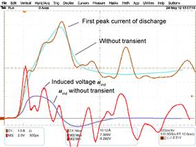
Figure 4 shows the first peak current of discharge of the ESD generator in magnified form. Several transients are clearly visible on the leading edge which are designated ESD transients in the following text. The discharge current peak and the ESD transient also produce a magnetic flux B1 (Figure 1) with an identical variation over time. The magnetic flux B1 induces a disturbance voltage uind (Figure 4) in a conductor loop of the electronic module. The conductor loop has a size of 8 mm2. The voltage set for the ESD generator is 2 kV. Furthermore, Figure 4 shows clearly that the largest voltage induction is generated by the ESD transient. The rise time of the discharge current peak of 0.7 to 1 ns as defined by the standard generates a lower disturbance voltage induction (Figure 4, curves without transient).
The ESD transient of the ESD generator has a stronger disturbance effect than the discharge current peak. The waveform parameters as defined by the standard are thus not suitable for comprehensively describing the disturbance effect of the ESD generator. Transients strongly depend on the type of ESD generator used in practice.
The fields B2 and B3 boost the disturbance effect of the ESD generator (Figure 1). Figure 5 shows the disturbance voltage induced by the field B2 in a conductor loop of 8 mm2. The voltage variation with time is totally different to the usual curve of the ESD events generally known. The 200 ps-wide spike has the largest disturbance effect on ICs. It has an amplitude of 4.8 V. This pulse was too short for slower ICs of the older generation and hardly caused any trouble at all. Modern, fast ICs can process this narrow pulse and suffer from malfunctions. What is special about this event, i.e. voltage induced by field B2, is it has nothing to do with the standard pulse. It occurs in addition to the actual test, which means that the standard test is no longer unambiguous.
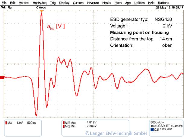
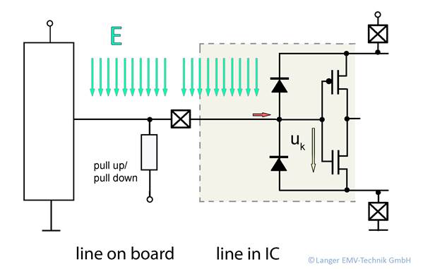
Figure 6 shows the operating principle behind voltage induction (equivalent circuit) via the magnetic field B of the ESD generator. The induction loop can be located outside the IC on the printed circuit board or inside the IC package. Outside it is formed by a trace closing to ground via a low-impedance driver in this example. The disturbance voltage enters the IC via the trace by conductive coupling. Within the IC, the induction loop is formed by pins, the lead frame and bonding wire. The voltage uind induced in the induction loop is present at the IC input. Both voltages, the internal and the external one, cause malfunctions inside the IC. The voltage uind depends on the rate of change of the discharge current and magnetic field of the ESD generator respectively. This correlation is described by the law of induction: uind = -d Φ / d t. The faster the rate of change of the disturbance, the higher the voltage induced. The burst generator according to IEC 64000-4-4 provides pulses with a rise time of 5 ns. The magnetic fields of the burst generator induce a lower voltage than the disturbance produced by the ESD generator. The ESD generator provides pulses with a rise time of 0.7 to 1 ns and induces a five-fold higher voltage with the same current value. The leading edge transients of the ESD generator have a rise time of approx. 200 ps. These transients will induce an even higher voltage.
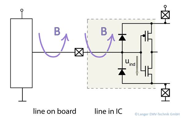
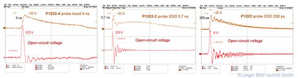
Figure 7 shows this correlation. The current shown here generates a magnetic field B that penetrates the conductor loop. The voltage uind is induced in the conductor loop. The disturbance events: burst, ESD, ESD transient induce different voltages. The width of the voltage pulse induced corresponds to the rate of change of current. Pulses with a width of 5 ns are produced during a burst event. ESD events generate pulses with a width of 1 ns and ESD transients produce pulses with a width of 200 ps. Modern ICs will also process pulses with a width of 200 ps which will then lead to IC malfunctions or even its total failure.
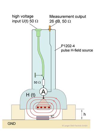
According to the law of induction, the value of the voltage induced is inversely proportional to the rate of change of the disturbance event. The measurements for Figure 7 have been carried out with defined field sources (Figure 8). These field sources have a fixed field generation geometry for different disturbances. The test current will thus always produce the same field coupling so that the results measured for the three disturbance events described can be compared. An IC can be subjected to the defined fields and its immunity tested in operation.
Switching voltages with a high rate of change occur at the high-voltage switch, current conductors and other components in the ESD generator during the discharge (Figure 2). These switching voltages generate electric fields with a high rate of change that couple from the generator housing to the device under test. Figure 9 shows the electric field which emerges from the rear part of an ESD-generator housing. Its rate of change is approx. 1 ns.
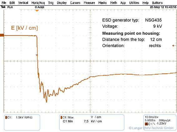
Figure 10 shows the equivalent circuit diagram and the operational principle behind the coupling in by the electric field of the ESD generator. The electric field couples into a signal line. The capacitive coupling between the affected signal line and the ESD generator is low. The value of this capacitance depends on the surface area of the signal line and is in the fF range for this coupling. The electric field of the ESD generator drives a capacitive current into the signal line. This current flows to ground (GND) via the pull-up resistor or the internal resistor of the connected driver. The current produces a voltage pulse at the resistor. This voltage pulse reaches the input of the IC and interferes with the IC. The peak value of the voltage pulse depends on the rate of change of the electric field, the pull-up resistance and the surface area of the signal line that is subjected to the field. The pulse width depends on the rise time. The faster the rate of change of the disturbance, the higher the voltage coupled in. The burst generator according to IEC 64000-4-4 provides pulses with a rise time of 5 ns. The electric fields of the burst event couple a lower voltage than the disturbance triggered by the ESD generator. The ESD generator provides pulses with a rise time of 0.7 to 1 ns and couples a five-fold higher voltage into the device under test. The highest rate of change of E fields from an ESD generator is approx. 200 ps. Due to these events, an even higher voltage is coupled into the device under test.
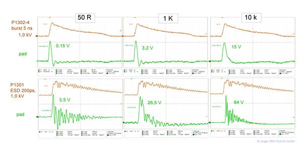
This electric coupling was investigated in experiments. A similar test set-up as shown Figure 8 was used for these experiments. An E field source was used to generate the required fields. Figure 11 shows the results. A 5 ns burst pulse and a 200 ps ESD pulse were used for the measurement. In addition, the dependence on the pull-up resistor (driver) used in the set-up was examined.
The voltage coupled into the IC is proportional to the pull-up resistance. The lowest voltage (0.15 V) is coupled into the IC at a rate of change of 5 ns and a pull-up resistance of 50 Ohm. This voltage will not yet interfere with the IC. The highest voltage is generated at a rate of change of 200 ps and a pull-up resistance of 10 kOhm and amounts to 64 V. Figure 11 shows that the 200 ps pulse can already cause malfunctions in the IC with a low-impedance pull-up (driver) resistance of 50 Ohm (with a voltage of 3.5 V). This makes this pulse particularly dangerous for electronic circuits since even the smallest sections of lines that are driven by a low impedance source such as a data bus, address bus, etc. can become a victim of interference on this way. The surface area of the size of a test pad on the respective line is sufficient to cause malfunctions in the IC. This problem is limited to modern, highly integrated ICs which are fast enough to process this type of pulse.
It is important for designers to know the immunity of the ICs that are planned to be used for a module with highly integrated circuits. Not all pins of an IC are equally sensitive to EMI. Usually there are just a few highly sensitive pins. These pins have to be identified so that appropriate and effective EMC countermeasures can be taken.
Signal lines should be routed in internal layers and shielded by GND planes on both sides to reduce interference effects from electric fields, for example. It has to be noted that the number of test pads and vias also has to be reduced.
Modern measuring techniques and test devices are available to determine the conducted and radiated immunity of ICs.