

EMC problems in the development of electronic modules for the automobile industry result in very high development costs and loss in time.
Automobile electronic systems have to comply with ever increasing demands on performance. This is why more and more highly-integrated, ESD-sensitive ICs are used in this field. Consequently, ESD faults lead to more and more malfunctions. These functional problems mainly affect highly-integrated micro-controllers where the oscillator cells and PLL cells react very sensitively to ESD processes. Today's electronic applications do not even achieve an ESD immunity of 2 kV in the worst case. Experience has shown that applications with a heat sink on the microcontroller are particularly sensitive (Figure 1).
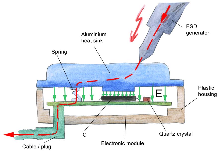
Im Figure 1 shows the operational principle behind ESD interference. The ESD generator couples a disturbance pulse into the heat sink. This results in a voltage difference between the heat sink and the electronic module. This voltage difference generates an electrical interference field between the two components. The electric field strength is the highest in the area of the heat sink since this is where it is closest to the IC. The distances are in the range of approximately 0.2 to 1 mm in practice. This high electric field strength may cause the IC to fail.
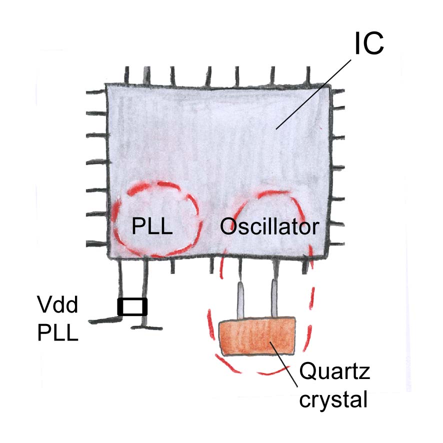
An examination of the IC with an electric field source that is guided by hand will reveal that the PLL and oscillator areas are particularly sensitive. A corresponding analysis of the IC faults confirms PLL and oscillator faults.
On the basis of the example in Figure 1, ESD immunities can be assigned to the respective fault patterns:
- 2 kV ESD for oscillator cells
- 3 kV ESD for PLL cells
A shield can be arranged over the IC to ensure that no electric fields interfere with the IC (Figure 3). This will intercept the electric fields emitted by the heat sink. The shield must also extend over the quartz crystal in the ESD test.
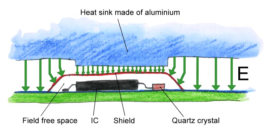
This precaution allows the ESD immunity to be increased to approximately 15 kV. It is not the shield that determines the 15 kV limit but further weak points in the electronic module. They are responsible for disturbances being coupled to the IC via the line networks simply by passing beneath the shield.
The ESD test can only be performed on a finished component. This means that the development and production of all parts of the component and the tools for its production have been completed. The usual way to achieve EMC immunity through changes to the circuit board layout does not lead to the desired goal in our example. ESD disturbances that originate from the heat sink act directly on the IC housing. The problem can only be solved by changing the mechanical design. This means that mechanical structural parts have to be changed and thus also the tools that have been used for their production. This is an expensive approach.
This problem can be avoided if the IC's EMC characteristics are known before its production.
There are two fields where action can be taken:
- the IC manufacturer can improve the IC. This has already been implemented in practice.
- appropriate EMC precautions can be planned in the mechanical structural design.
Measurements are necessary to determine the EMC characteristics of ICs.

Figure 4 shows a measurement set-up to measure the E-field sensitivity to ESD pulses with an ESD generator. An electrode is arranged over the IC for this purpose onto which the tip of the ESD generator is placed. A corresponding electrical pulse field is generated between the electrode and the test board when an ESD pulse is applied. The IC's immunity level can be determined by increasing the voltage of the ESD generator. This procedure is not very precise since the electric field pulse largely depends on the type and position of the ESD generator . The pulse edges of the ESD generator can superimpose with ESD-generator-specific transients, for example. The waveform of the pulse can also change by inclining the ESD gun, for example. Furthermore, a stray field may emerge from the generator and uncontrollably interfere with the IC. Further variations and similar phenomena are possible .
Figure 5 shows a defined procedure.
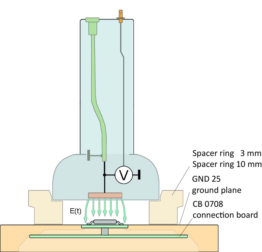
During the test, the IC is located in a shielded space that is formed by the ground plane, spacer ring and field source. The field source is arranged over the IC at a defined height using the spacer ring. The field source includes an electrode to which the test voltage pulse is applied. The electrode generates a defined electric field in which the IC is located. The field source can be used to generate a wide variety of test pulses that may occur in practice. Rise times of 200 ps, 1ns and 5ns may occur in actual use. The electrode voltage is increased until the IC's immunity level is reached.
During the ESD event, structural parts may generate additional magnetic fields which may also interfere with the IC in practice. The same measurement set-up and a magnetic field source can be used to determine the IC's magnetic field immunity level. The IC's fault patterns have to be analysed during these measurements. Table 1 lists the results of ESD immunity measurements for a microcontroller as a function of the disturbance pulse rise time.
| 200 ps | 1 ns | 5 ns | |
|---|---|---|---|
| E | 1,4 kV | 1,8 kV | 6,0 kV |
| H | 2,8 kV | 3,0 kV | 7,0 kV |
| Table 1 | |||
The measurement set-up that is described here allows the EMC parameters of an IC to be determined. The measurement results can be used to plan corresponding structural design modifications for IC.
Changes to the layout as a countermeasure are inappropriate if electric or magnetic fields interfere with the IC from outside. The only helpful remedy is to change the mechanical design in this case.
The following countermeasures can be taken for the concrete example in Figure 1, where a heat sink over an IC generates a strong electric field:
- increase the number of contact springs between the electronic module and the heat sink
- arrange a local shield over the IC, Figure 3
- enclose the module with a shielding housing on all sides if possible (perhaps with a feedthrough filter)
- move the IC to the side where no field occurs (cooling will not be possible)
- increase the gap between the IC and heat sink
Item 1) The contact springs reduce the voltage difference between the heat sink and the printed circuit board. This is due to the fact that the springs' total inductance is reduced if several springs are arranged in parallel. It may be necessary in practice to install approximately 20 springs to achieve this objective. The springs' magnetic stray field may interfere with the IC if they are arranged in unfavourable positions. Complex and comprehensive tests are thus necessary to determine favourable spring positions. However, a reliable spring contact cannot be ensured if an aluminium heat sink is used. This means that the aluminium heat sink would also have to be tin-plated, something that entails high costs. An IC shield may be more cost-effective at this point (see item 2).
Item 2) When arranging a local shield above the IC, it has to be ensured that this also covers the quartz crystal (similar to Figure 3). However, the quartz crystal can also be placed in an area which is free of fields on the other side of the electronic module, for example.
Furthermore, it has to be ensured that the shield component is suitable for the manufacturing process.
Item 3) The metal shielding should enclose the entire module if possible. This may hamper the use of plastic housings.
Item 4) The IC can be moved to areas where no fields occur, on the other side of the electronic module, for example, if the IC does not necessarily have to be cooled. In this case it should be noted that web-like structural metal parts that exist there may couple out magnetic fields which could interfere with the IC too. The test of the first sample will show whether the modification of the entire design to this end has been be successful, which is rather late in the production process.
Item 5) The theoretical possibility of increasing the gap between the heat sink and the IC would cause a reduction in the electrical field strength. At the same time, the heat transfer and thus the cooling effect on the IC would deteriorate.
In summary, it can thus be said that, in terms of time and cost savings for the development of a component that is immune to interference, it is very beneficial to know the ESD parameters of the microcontrollers in advance. This means that the ESD parameters of the microcontrollers have to be measured. The information will allow necessary countermeasures to be planned as early as during the component's development in order to ensure that the whole component is immune to interference.