

These are relatively harmless phenomena. Much more serious problems could occur that may even jeopardise driving safety or impair the car's functions.
High-frequency interferences are very tricky in modern electric automobiles, hybrid vehicles or complex electronic systems for the driver's safety and comfort.

Usually, it is not an electronic component as a whole but an individual device that is responsible for emissions. The device, such as a quartz crystal resonator or microcontroller, causes local electromagnetic fields that induce voltages in housings or structural parts. These parts are thus stimulated to oscillate and, as a result, radiate emissions. The developer will certainly check his components for emissions by carrying out component measurements in an EMC test chamber during the development process. But these will measure emissions from the device under test in general. The measuring methods used in such tests are unable to sufficiently assess the near fields of a device under test. When performing measurements with conventional methods, the developer cannot intervene directly in the device under test, measure individual sections of the component more precisely or do anything to get to the bottom of the emissions source. He takes his device under test out of the EMC chamber, puts it in its package and takes it back to his workplace. Another problem in conjunction with these component measuring methods is that the component is tested outside its actual vehicle environment and emission frequencies may possibly not be measured since the otherwise present neighbouring structural parts are not stimulated to oscillate.
Back at his workplace, the developer can only compare the frequency images from the component test with those gained from experiences in other development processes and make assumptions about the reasons behind the problems. He will then modify the device under test on the basis of these assumptions. Only further test measurements in the EMC chamber will show him whether this was correct and successful. The measurement set-up has to be repeated for new component measurements. But in most cases the component, and especially the cable harness, cannot be returned to an absolutely identical position. This results in measurement deviations. The frequency response characteristics measured at the different development stages of the device under test cannot be compared immediately and flexibly. The developer has to place individual protocols one beside the other and compare them step by step.
This approach to EMC component development takes a lot of time, is complicated and unsatisfactory for the developer - it thus requires a lot of effort and causes high costs.
What is needed here is a more effective search for emission sources in complex electronic systems during the development. The engineer must be able to measure as many disturbances as possible, systematically identify RF sources, carry out modifications and tests flexibly at his workplace in order to save time and costs.
Let us now take a look at how a component may become a source of emissions.
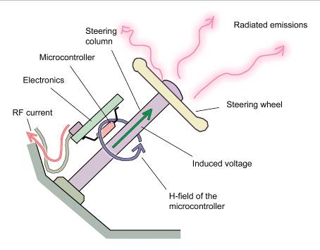
An electronic assembly or a printed conductor itself does not usually send out any emissions. But individual devices may generate RF near fields and these encircle connected cables, for example. They induce a voltage there and thus cause them to radiate emissions. Due to electric or magnetic coupling (i.e. in the near field), the entire metallic system, comprising the component and its connected cables as well as metallic parts such as housings, shielding plates, etc. in its immediate vicinity, is subject to "self-excitation" (figure 2).
The metallic system in its entirety acts as an antenna when excited by the electronics. The "RF exciting current" from the electronics to the antenna (cables and metal parts) can thus be assumed to be an approximate measure of the emissions from the device under test.
We will now describe a measurement set-up that complies with our requirements for the efficient development of a component in terms of emissions.
Emissions are measured under conventional measurement conditions with an antenna, for example. The device under test must be modified if one or more frequencies of the development sample exceed the limit values defined in the respective standard. The values from this measurement are used as a reference for subsequent comparative measurements (figure 3).
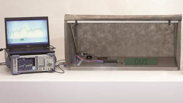
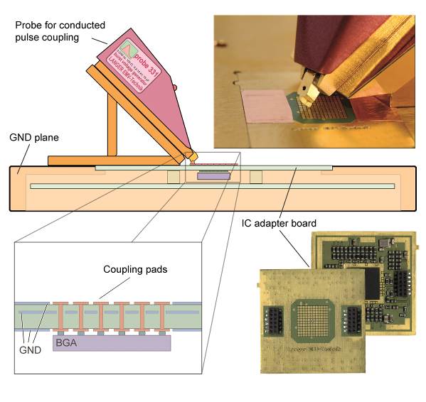
When measuring emissions from electronic systems at a developer's workplace, it is important to define a measurement set-up that simulates the component's environment in the passenger compartment as closely as possible. A confined measurement set-up is arranged at the workplace to measure all reasonable RF currents of the device under test. Should the relevant frequencies be in a range that is subject to high external interference from the environment such as radio frequencies, a shielding tent is used to protect the measurement set-up against this interference. This shielding tent has a footprint of 50x90 cm and an attenuation of more than 40 dB in the frequency range from approx. 80 to 650 MHz. The front of the shielding tent can be folded up and down. The entire shielding tent can be opened wide to allow easier modification of the device under test. Supply lines such as power supply, cables for transmitting measurement signals are led to the outside through filtered bushings in the ground plane. This also establishes a fixed ground reference for the device under test and parts of the measuring equipment.
How is the measurement carried out at the developer's workplace?
A comparative measurement is carried out with the RF current transformers in the closed shielding tent and documented in a first step. These measurement results are compared with the results from the component measurement to confirm the measurement set-up. Of course, the measurement results will not coincide. But it is important that the relevant frequencies from the component measurement are also found in the frequency image of the measurement set-up that has been chosen.
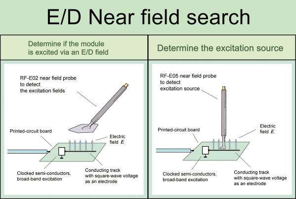
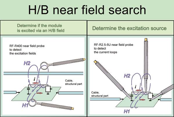
In the next step, magnetic field and/or electrical field probes are used to scan the ICs, line connections, plug-in connectors, etc. A precise analysis of the frequencies and the orientation of the near fields often allows the developer to recognise the correlations between the fields and the exciting currents. The front of the shielding tent must be opened to measure the near fields with the probes. Of course, the shielding effect is then much lower than when the shielding tent is closed. The near fields of the device under test, however, are usually much stronger than the fields coupling in from the environment so that measurements can nevertheless be carried out successfully. The intensity of the field at a certain frequency and/or within a certain frequency range. figure 4 and figure 5
- electrical fields above devices such as processors
- electrical fields on switched lines and bus systems
- magnetic fields on switched data and clock lines
- magnetic fields at power supplies
As soon as the RF sources have been identified, the board can be modified on site by soldering components in place, taking shielding measures or rerouting lines. The results of a further measurement with the RF current transformer in the closed shielding tent will immediately show whether the measure that has just been taken is effective or not. RF current transformers and near-field probes can be used alternately for measurements in subsequent tests. The component can be constantly modified until a minimum exciting current from the RF current transformer flows in the supply line.
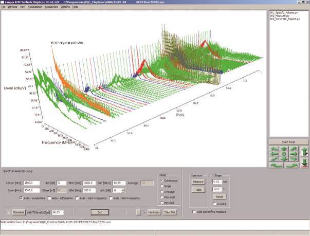
The frequency response characteristics that are measured can be documented with a PC and customized software. This software allows the developer to record, colour, annotate, calculate and visualize any number of curves of a spectrum analyzer and it enables a flexible, easy and fast comparison of the different steps of the measurement process. The developer can simply export images and data from the software for documentation and statistical analysis (figure 6).
A closer look at EMC problems of components shows that plug-and-socket connectors A closer look at EMC problems of components shows that plug-and-socket connectors, and in particular connectors used in the HV systems of hybrid automobiles, are special. They are subject to high demands in terms of EMC. Testing such connectors in the component's prototype is in fact too late since the developer has no chance of improving the connector. The developer should thus test the individual connector in terms of its EMC characteristics at the beginning of the development process or rely on connectors with known EMC parameters that are deemed sufficient for the component.
Apart from devices with one or two cable connections, complex devices can be tested too. At the beginning of the test, different effects caused by different RF sources within the device under test will superimpose and lead to an amplification or partial cancellation of RF fields at individual frequencies. It is therefore important for an efficient analysis of the causes, especially in complex devices under test consisting of several printed circuit boards, that the device be dismantled to manageable parts and the individual printed circuit boards be investigated separately.
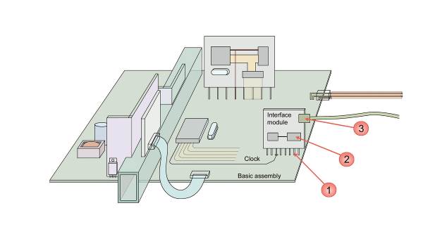
The device under test shown in Figure 8 has several potential emission sources. The investigation is limited to the interface module of the component in this example.
Three RF sources are conceivable:
- the connector between the basic assembly and the interface module
- the electronics (PHY with a microprocessor) on the interface module
- the connector of the interface cable
These three RF sources will now be dealt in succession. This requires measurement set-ups that suppress the respective other RF sources and the RF sources of the basic assembly as far as possible.

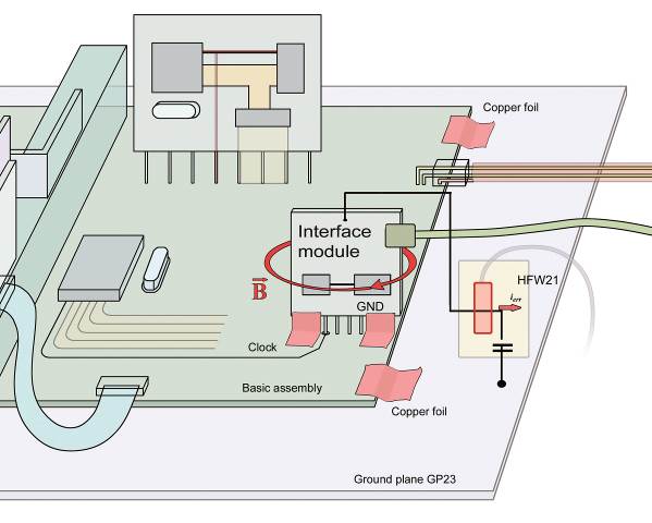
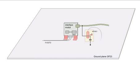
1) Connector between the basic assembly and the interface module (figure 9 )
The basic assembly and interface module are connected to each other via data and control lines. These lines are well protected on the printed circuit board in the area of the basic assembly and the interface module since they are embedded into ground surfaces. But in the area of the connector they pass freely through an open space. The signal currents in the lines generate RF magnetic fields which propagate inside and around the connector. They generate induction voltages in the connector's ground pins. As a result, there is a voltage difference between the basic assembly and the interface module. This drives an RF current into the interface cable via the interface board which in turn causes an excitation of the cable and thus emissions from it.
A COM port of the current transformer is connected at a short distance to GND of the interface module to measure the current that is driven by the induction voltage. The current measured with the current transformer is a measure of the connector's share of the total emissions from the device under test. The effect of modifications such as filters on signal lines or changing the pin assignment can be measured directly.
2) Electronics (PHY with a microprocessor) on the interface module (figure 10)
The ICs of the interface module generate currents that flow into the GND system where they induce a voltage. This voltage in turn drives a current from the basic assembly through to the connected interface cable which excites the interface cable to send out emissions.
The basic assembly remains connected to the ground plane during the measurement. The connector's share in the emissions between the ground plane and the interface module is cancelled out by several large-area GND connections. The voltage that is induced by the IC currents can be picked up with the current transformer at the upper end of the assembly. The current transformer measures a proportional current. Modifications that are carried out directly on the interface module can thus be assessed.
3) Connector of the interface cable (figure 11)
The interface connector is another RF source in this complex component. During data transfer the interface driver drives a current through the connector. This current induces a direct-axis voltage in the connector housing that stimulates emissions from the interface cable.
The current transformer is connected to the interface cable for the measurement.
It has to be noted that the voltage is superimposed according to number 2 above during this measurement. This voltage can be short-circuited by gluing a piece of copper foil to the interface circuit board.
The integrated circuit is another electronic element that is important for the developer of the component. The characteristics of the ICs used for the electronic system have a major influence on the EMC characteristics of the entire component. The structures of microcontrollers and chipsets are becoming increasingly smaller. This is why the IC's sensitivity today can be up to ten times higher than that of their predecessor models. The behaviour of ICs and their package types in terms of immunity and emissions is a crucial aspect which the developer has to take into account when choosing devices for a component. It is thus important to select an appropriate IC and use it in compliance with the respective EMC requirements in the planning phase of a component's development process. Compliance measurements according to BISS/IEC should be carried out on ICs with respect to EMC parameters as a standard procedure. But these measurements are not enough to ensure that an IC is successful in practice. In addition, ICs should be tested with practical and universal EMC parameters such as ESD (Langer EMC parameters, data on request).
The pulses that occur on ICs during ESD and burst tests for devices can be simulated for IC immunity tests. Special IC measuring and testing technology should allow the developer to carry out immunity tests independent of the device or component (figure 12)
The developer has to delve deep into a component's physical process during IC emissions analysis. If, for instance, a fast circuit with its high-frequency currents and voltages is placed in an unfavourable position on the device, this may interfere with the component itself or other components or devices through coupling paths via the component.
The test results help achieve three objectives:
- Improvement of the IC to avoid problems in later use,
- Practical parameters and conditions for the interference-free use of the IC on components and
- 3. Selection of an IC that is suitable for the IC user's application on the basis of the IC's EMC parameters provided by Langer.
Procedures and information are thus available to the electronics developer that help him plan the EMC of a complex component in advance and to measure and modify this directly at his workplace during the development process. Development becomes more efficient and less time-consuming. Fewer component tests in an EMC chamber will be necessary. This reduces lengthy waiting times whenever an EMC chamber has to be used. This in turn speeds up component development so that resources, time and costs can be saved.