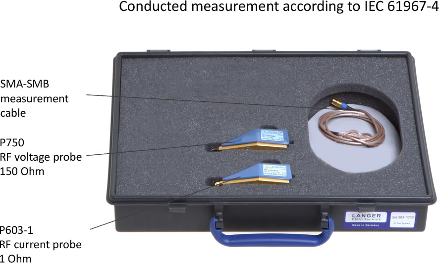

User manual
P603-1 / P750 setRF conducted measurementaccording to IEC 61967-4
1 General description
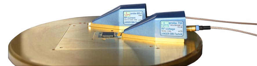
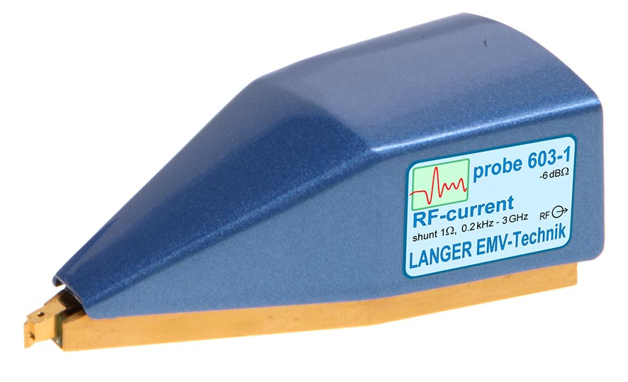
The P603-1 and P750 probes have been developed to measure conducted emissions from integrated circuits (ICs) with direct 1 Ohm/150 Ohm coupling. The probes can be used to perform measurements on ICs according to IEC 61967-4 (Figure 1). The P603-1 probe corresponds to the 1 Ohm RF current probe head.
The P750 probe corresponds to the impedance matching network according to IEC 61000-4-6. It has an input impedance of 150 Ohm.
The P750 probe can be used to perform RF voltage measurements and the P603-1 probe can be used for RF current measurements on IC pins.
The P603-1 and P750 probe can also be used for other measurement tasks:
- Current measurement (P603-1) on concatenated Vdd pins, Figure 2
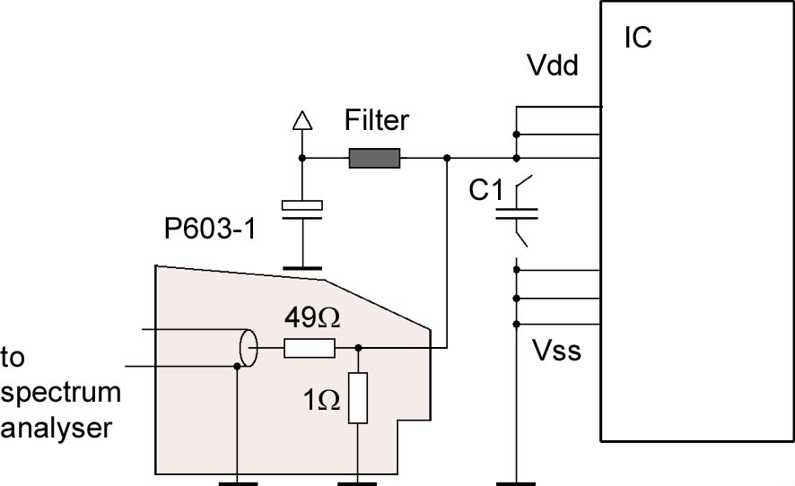
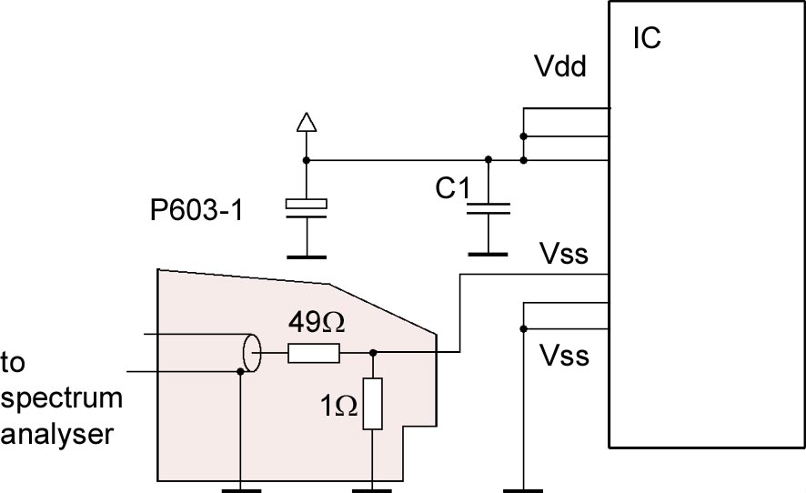
- Current measurement (P603-1) on a single Vss pin, Figure 3
- Current measurement (P603-1) on a single Vdd pin, Figure 4
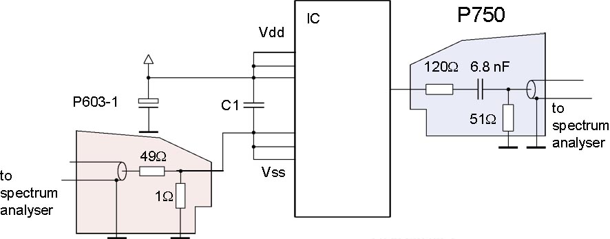
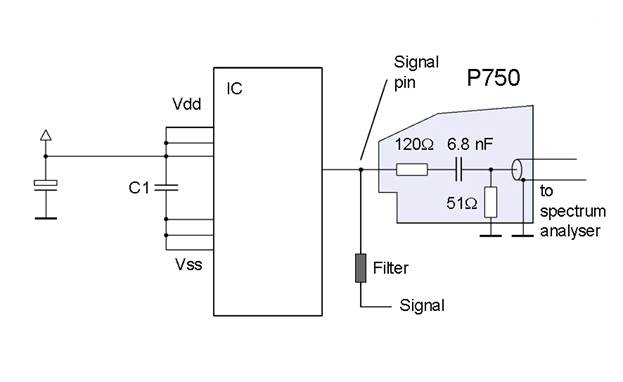
- Voltage measurement (P750) on a signal pin while this is in operation, Figure 5
- Current measurement (P603-1) on a signal pin while this is in operation, Figure 6
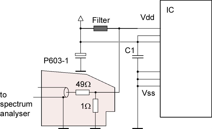
- Voltage measurement (P750) on a Vdd or Vss pin, Figure 7
An 80 µF capacitor is integrated into the P603-1 probe as a direct current block. It backs up the IC in the circuit diagrams Figure 2 and Figure 4.
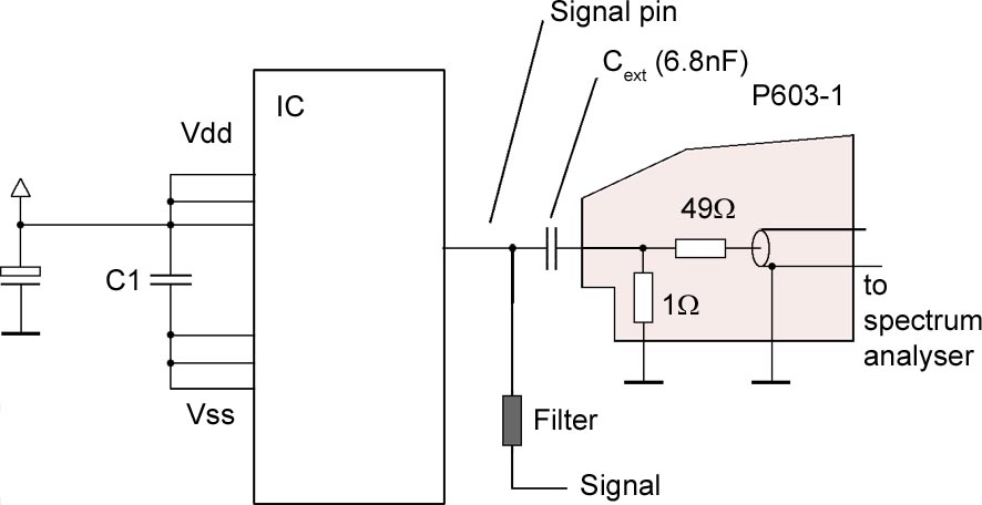
The external capacitor Cext can reduce the stress on the signal pin caused by the probe's low impedance (1 Ohm) (Figure 6) during current measurements on signal pins.
The impedance of the capacitor Cext should be at least 3 dB smaller than the shunt's 1 Ohm resistance.
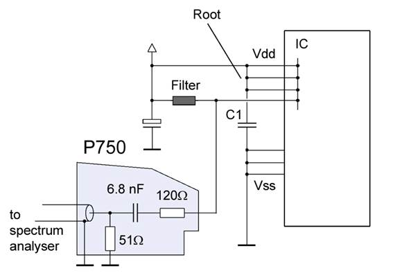
An IC internal connection to other Vdd supply pins is assumed for a voltage measurement on a Vdd pin (Figure 7). This measurement enables the determination of voltage dips on the IC's internal Vdd network.
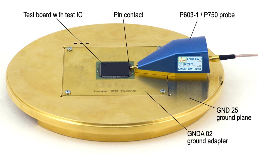
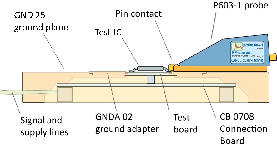
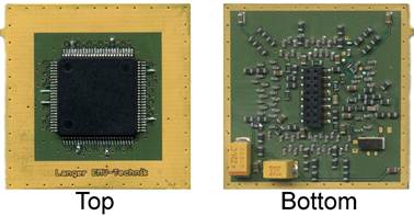
The test IC is soldered to the test board (Figure 8). The P603-1 and P750 probes can be moved freely on the GND 25 ground plane or GNDA ground adapter (Figure 8). Unlike the measurement set-up according to IEC 61967-4, this set-up ensures that the P603-1 or P750 probe's pin contact can reach and contact each IC pin. The probes are fixed on the ground plane with magnets. Filter elements and bridges are located on the underside (bottom) of the test board to prepare the measurement set-up for contact with the probe (Figure 10).
The same test board is used for all measurement methods (1 Ohm, 150 Ohm). Bridges are provided to the Vdd / Vss root at the Vdd / Vss pins in the initial state. The associated bridge to the root is removed and the corresponding filter becomes active if a Vdd / Vss pin is measured.
2 P603-1 probe
2.1 General Description
The P603-1 probe is an RF current probe head to measure conducted RF currents on IC pins according to IEC 61967-4.
The P603-1 has been designed for measurements on supply (Vdd / Vss) and signal pins. The measurement is performed with a 1 Ohm shunt.
2.2 Design and function of the P603-1 probe
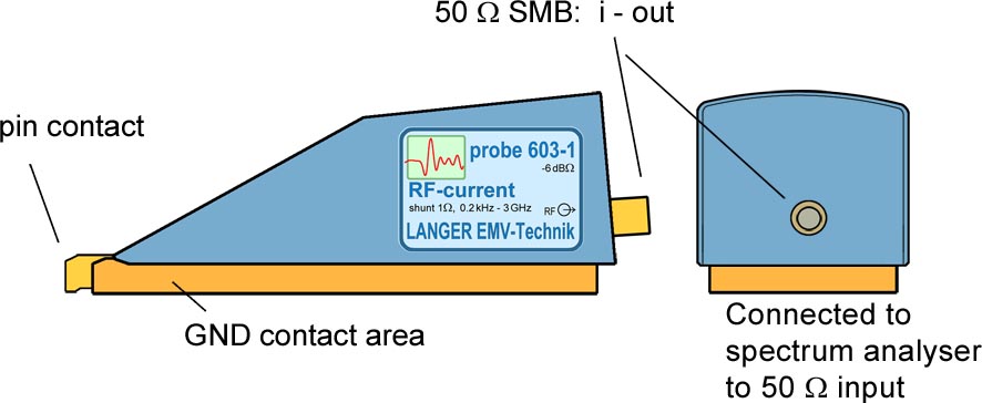
The P603-1 probe contains a 1 Ohm current probe head (IEC 61967-4). The input of the current probe head is connected to the probe's pin contact (Figure 12). The output of the current probe head is connected to the 50 Ohm SMB port at the rear end of the probe.
A cable is used to connect the probe's output to a measuring instrument such as a spectrum analyser. The voltage measured is equivalent to the current measured.
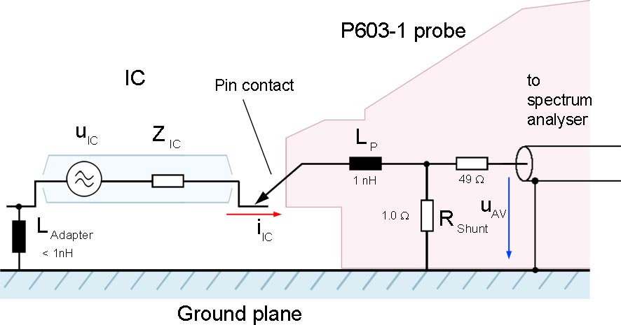
Figure 13 shows the equivalent circuit diagram of the P603-1 probe. The current probe head comprises a 1 Ohm shunt, 49 Ohm matching resistor and 80 µF coupling capacitor.
The capacitor Ck (IEC 61967-4 direct current block) disconnects the direct current between the test IC and the probe. An additional capacitor Cext can be inserted between the test IC and the probe to reduce the stress on the signal pins caused by the 1 Ohm shunt. The P603-1 current probe head has an inductance LP of 1 nH in the line from the tip of the probe contact to the shunt. This value and the associated measurement error are much smaller than the value achieved with the set-up according to IEC 61967-4.
The pin contact of the probe has to be brought into contact with the respective test IC pin to perform the measurement. Please refer to the “ICE1 user manual” and “IC test instructions”.
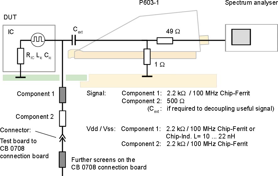
Figure 14 shows the design of the Vdd / Vss and signal pin filters which are located on the bottom of the test board. Please refer to the “IC test instructions” for a guideline on how to set up a test board.
3 P750 probe
3.1 General Description
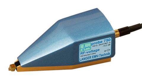
The P750 probe is a matching network to measure conducted RF voltages on IC pins according to IEC 61967-4.
The P750 has been designed for measurements on supply (Vdd / Vss) and signal pins. The measurement is performed with a 150 Ohm voltage divider.
3.2 Design and function of the P750 probe
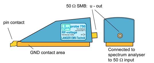
The P750 probe contains a 150 Ohm matching network (IEC 61967-4). The input of the matching network is connected to the probe's pin contact (Figure 16). The output of the matching network is connected to the 50 Ohm SMB port at the rear end of the probe.
A cable is used to connect the probe's output to a measuring instrument such as a spectrum analyser.
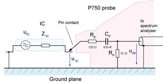
Figure 17 shows the equivalent circuit diagram of the P750 probe. The matching network comprises a 120 Ohm – 51 Ohm voltage divider and a 6.8 nF coupling capacitor.
The pin contact of the probe has to be brought into contact with the respective test IC pin to perform the measurement. Please refer to the “ICE1 user manual” and “IC test instructions”.
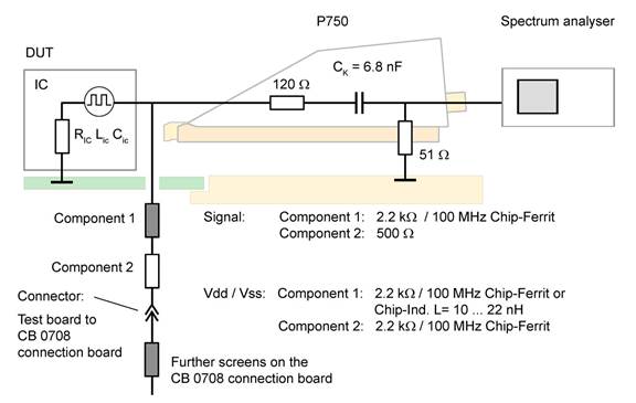
Figure 18 shows the design of the Vdd / Vss and signal pin filters which are located on the bottom of the test board. Please refer to the “IC test instructions” for a guideline on how to set up a test board.
4 Measurement set-up
4.1 Performing the measurement
Figure 19 shows the measurement set-up to measure conducted emissions from integrated circuits (ICs). The test IC is mounted on the test board. The test board is inserted into the corresponding ground adapter such as GNDA 02. The signal and supply connections to the test IC are established through a plug connector on the test board. The test IC is supplied via the test board and controlled via the connection board. The associated Connection Board Control software can be used to control and monitor the test IC from a PC.
The GNDA 02 ground adapter is included in the ICE1 IC test environment. www.langer-emv.com
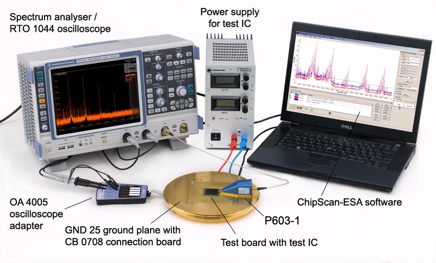
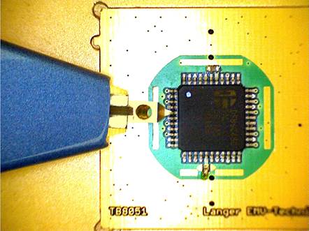
The P603-1 or P750 probe is placed on the GND 25 ground plane with the GNDA 02 ground adapter. The respective pin of the test IC can be contacted with the pin contact by moving the probe manually. The microscope camera (Figure 19) optically detects if and when contact is made. The camera's image is displayed on the PC monitor via the ChipScan-ESA software (Figure 21). The video image on the PC monitor enables the user to assess the connection to the respective IC pin. The spectrum analyser displays the RF signal that occurs if and when contact is made. The pins of the test IC can also be contacted automatically if an ICT1 automatic IC tester is available. The ICT1 automatic tester enables automatic measurements.
The AV input of the spectrum analyser is connected to the SMB output of the probe via an SMA-SMB 1 m RF cable.
The ChipScan-ESA software makes it easy to perform and document the measurements (see also: “ChipScan-ESA operating instructions”).
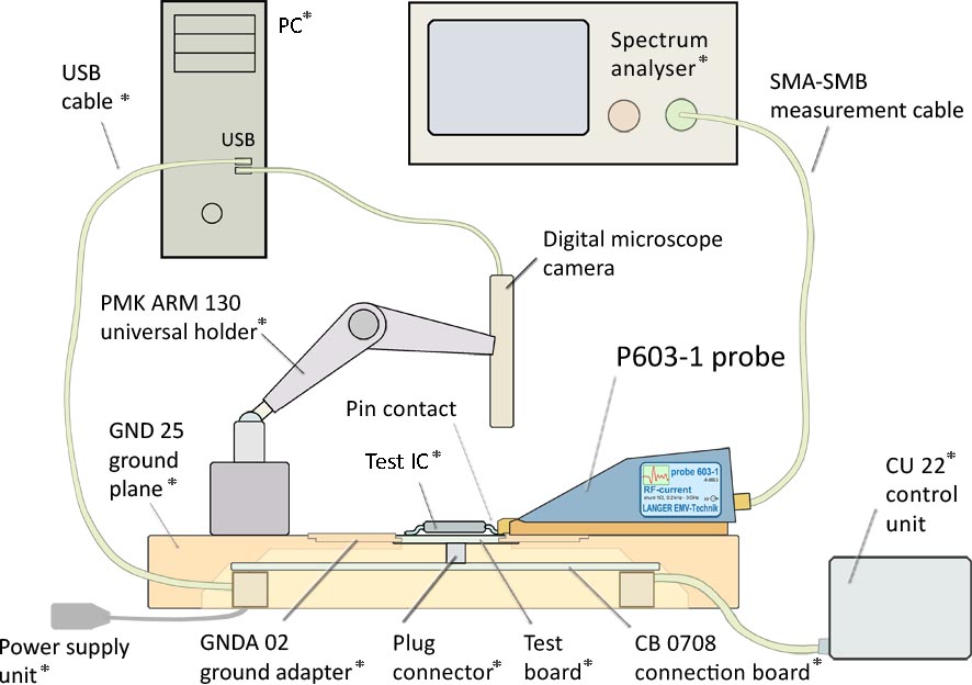
Components marked * are not included in the scope of delivery of the "P603-1 and P750 RF conducted emissions IEC 61967-4" probe set.
4.2 Using the ChipScan-ESA software
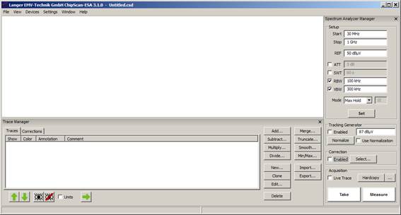
The spectrum analyser is sought automatically with "Devices/ Devices Manager/ Detected Devices" via the respective interface and connected to the PC (Figure 23).
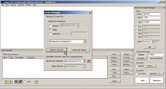
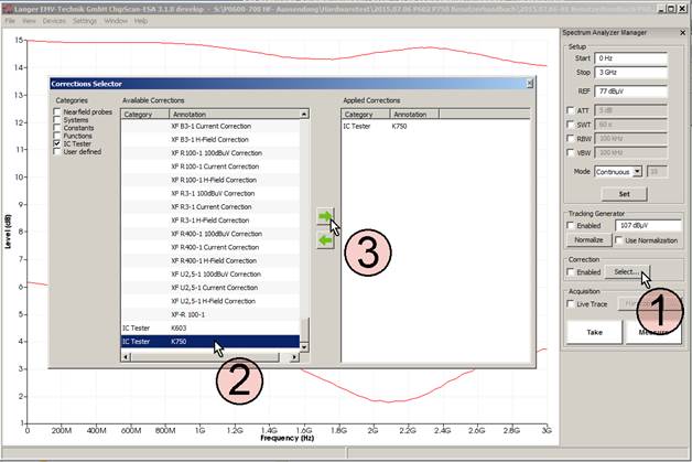
The main settings of the spectrum analyser have to be defined in the "Spectrum Analyser Manager" (Figure 23). The correction curve K603-1 or K750 has to be used to correct the frequency response of UAV(ω) measured with the P603-1 or P750 probe. UAV(ω) can be converted to IIC(ω) and UIC(ω) automatically under "Correction" in the "Spectrum Analyser Manager". The correction curve K603-1 or K750 has to be used for this purpose.
Mathematical functions can also be used (Figure 24): division by ω in the time domain, for example. This corresponds to a subtraction of 20 Log ω in the logarithmic form.
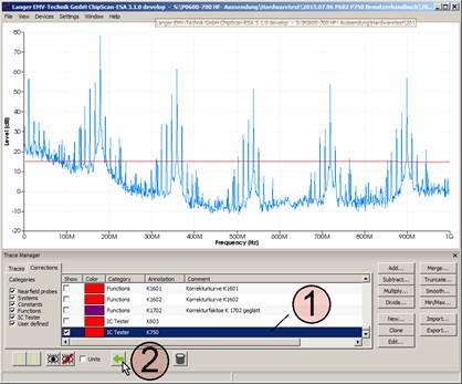
You can find the correction curve (-20 Log ω) in the "Corrections" list of the "Trace Manager".
Click the "Select" button (mouse cursor ① Figure 24) under "Correction" in the "Spectrum Analyzer Manager" to select the respective correction curve.
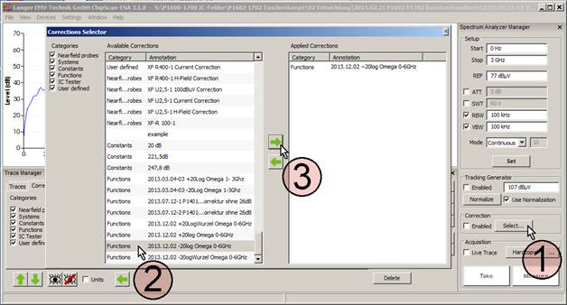
The "Corrections Selector" window opens Figure 24. Click and activate the correction curve -20 Log ω with the mouse cursor ②. Click the "Arrow right" ③ button to move the correction curve to the "Applied Corrections" list. Other correction factors and correction curves (Figure 25) such as K603-1 or K750 can be loaded in the same way or selectively (Figure 25).
The correction curve K603-1 is loaded to the "Corrections Selector" if the P603-1 probe is used for the measurement. Activate the "Enabled" box in the "Correction" field in the "Spectrum Analyzer Manager" with the mouse cursor ① (Figure 26). The field ② flashes if the correction is active Figure 26. Click "Take" or "Measure" (mouse cursor ③ Figure 26) to transfer the current measurement curve ④ IIC(ω) from the spectrum analyzer to the PC. The calculation: IIC(ω) = UAV(ω) + K603-1 is automatically performed at the same time. The curve IIC(ω) is added to the bottom of the "Traces" list in the "Trace Manager". A measurement log can be kept in the free text field under "Comment".
Delete the check mark from the "Enabled" box if you only want to measure UAV(ω); the field ② then stops flashing.
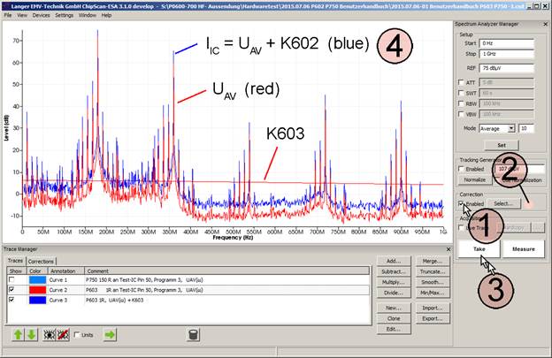
The "Curve" number is counted automatically (Curve 3) under "Annotation". The measurement log can be kept in the respective free text field under "Comment".
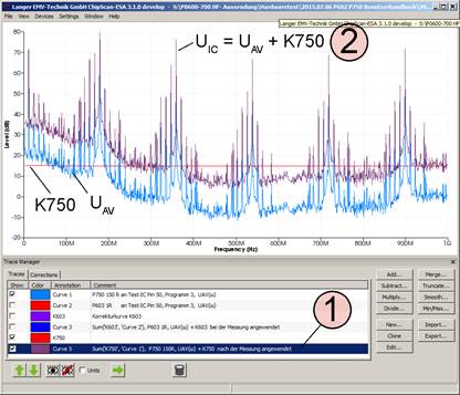
The correction can also be made later on if the measurement has been carried out using the P750 probe without any correction. The correction curve UIC(ω) = UAV(ω) + K750 has then to be added.
You can find the correction curve K750 in the "Corrections" list of the "Trace Manager".
Click the "Select" button (mouse cursor ① Figure 27) under "Correction" in the "Spectrum Analyzer Manager" to select the respective correction curve.
Mark the "Curve 1" (UAV) curve and the "K750" curve in the "Traces" list Figure 28 in the "Trace Manager" with the mouse cursor ①. Open the mathematical operation "Add…" (addition) and activate "Sum up all Plots" (Figure 28 mouse cursor ③). Click OK ④ to perform the addition UAV + K750.
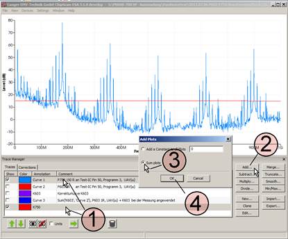
The calculation creates the entry (① Figure 29) at the bottom of the "Traces" list and is displayed as "Curve 5" (② Figure 29).
The user manuals for the respective devices are listed in the following table:
| Task | Operating instructions |
|---|---|
| IC test guideline (Langer EMV-Technik GmbH) |
| ICE1 user manual |
| Table 1 | |
5 Safety instructions
This product complies with the requirements of the following European Community Directives:
2014/30/EU (Electromagnetic Compatibility) and 2014/35/EU (Low Voltage)
When using the LANGER EMV-Technik GmbH product please observe the following basic safety instructions to protect yourself against electric shock and the risk of injury:
- Read and comply with the operating manual and keep the it in a safe place for subsequent use.
- Only personnel who are qualified in the field of EMC and fit for working under the influence of disturbance voltages and magnetic as well as electric fields may use the device.
- Follow the safety instructions and warnings on the unit.
- Always perform a visual check of the LANGER EMV-Technik GmbH product before use.
- Do not leave the LANGER EMV-Technik GmbH product unsupervised.
- Read the explanation of the symbols on the unit in the operating manual.
- The LANGER EMV-Technik GmbH product is only in use in applications it has been designed for. Any other use is not permitted.
- Do not switch the LANGER EMV-Technik GmbH product on until it has been completely assembled.
- Damaged connection cables must be replaced!
Attention: Function-related near fields and disturbance emissions may develop, particularly in connection with a test set-up while operating the product of the LANGER EMV-Technik GmbH. The user is responsible for measures to ensure that the intended use of products which are installed outside the companys EMC environment is not adversely effected (particularly by disturbance emission).
6 Safety instructions
Langer EMV-Technik GmbH will remedy any fault due to defective material or defective manufacture, either by repair or by delivery of replacement, during the statutory warranty period.
This warranty is only granted on condition that:
- the information and instructions in the user manual have been observed.
The warranty will be forfeited if:
- an unauthorized repair is performed on the product
- the product is modified
- the product is not used according to its intended purpose.
7 Technical specifications
7.1 P603-1 probe
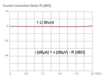
| Shunt | 1 Ω |
| Transfer factor Vout / Vin | -6 dB |
| Current correction factor R | -6 dBΩ |
| Max. power dissipation shunt | 2.5 W |
| Inductance of RF input | 1 nH |
| RF measuring output | 50 Ω (SMB) |
| Frequency range | 0.2 kHz – 3 GHz |
| Characteristics of the probe P603-1 | |
|---|---|
 | Figure 30 P603-1 characteristic |
7.2 P750 probe
| Transfer factor Vout / Vin | -15.2 dB |
| Frequency range | 150 kHz to 3 GHz |
| Input resistance | 150 Ω |
| Max. input voltage for RF | 3.5 V |
| Max. input voltage for DC | 50 V |
| RF measuring output | 50 Ω (SMB) |
| Characteristics of the probe P750 | |
|---|---|
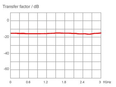 | Figure 31 P750 characteristic |