

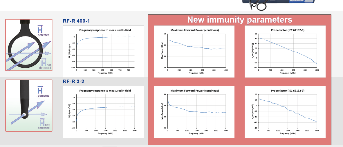
RF immunity testing with near-field probes for RF injection
The near-field probes of the RF Basic Set are now specified for RF injection. With the new immunity parameters, we are expanding the range of applications for these probes by adding a clearly defined area of use in RF immunity testing.
The graphics shown in the flyer present the corresponding near-field probes of the RF Basic Set together with the new immunity parameters. This provides users with a concrete basis for evaluating the level of power that can be injected into each probe continuously over a longer period of time and how the corresponding probe factor according to IEC 62132-9 (Immunity Scan of ICs) must be taken into account.
The first parameter describes the maximum power that can be continuously injected into the probe over a longer period of time. The second parameter is the probe factor according to IEC 62132-9. In combination with the illustrated curves, this shows that the release is not formulated only in general terms, but is based on specifically defined parameters for the respective probes.
For users, this means greater confidence when selecting and using near-field probes for RF injection. The new information provides clear guidance for practical use and makes it easier to classify the respective probe within the test setup.


Guest article: Troubleshooting Screen Blackout in a Large Industrial Drive System
Dr Min Zhang is a UK-based EMC consultant and founder of Mach One Design, specialising in EMC design, troubleshooting, and training. He holds a PhD in Electrical Engineering from Newcastle University and has a background in power electronics and motor drive systems. Formerly an EMC specialist at Dyson, he now supports companies worldwide and serves as Chair of the IEEE EMC UK & Ireland Chapter. He is also widely recognised for his popular YouTube channel, where he shares practical EMC insights and demonstrations.

Recently, a client experienced a nuisance issue with their product in the field. The problem was described as an occasional human–machine interface (HMI) screen blackout. As the issue occurred intermittently, it was suspected to be EMI-related.
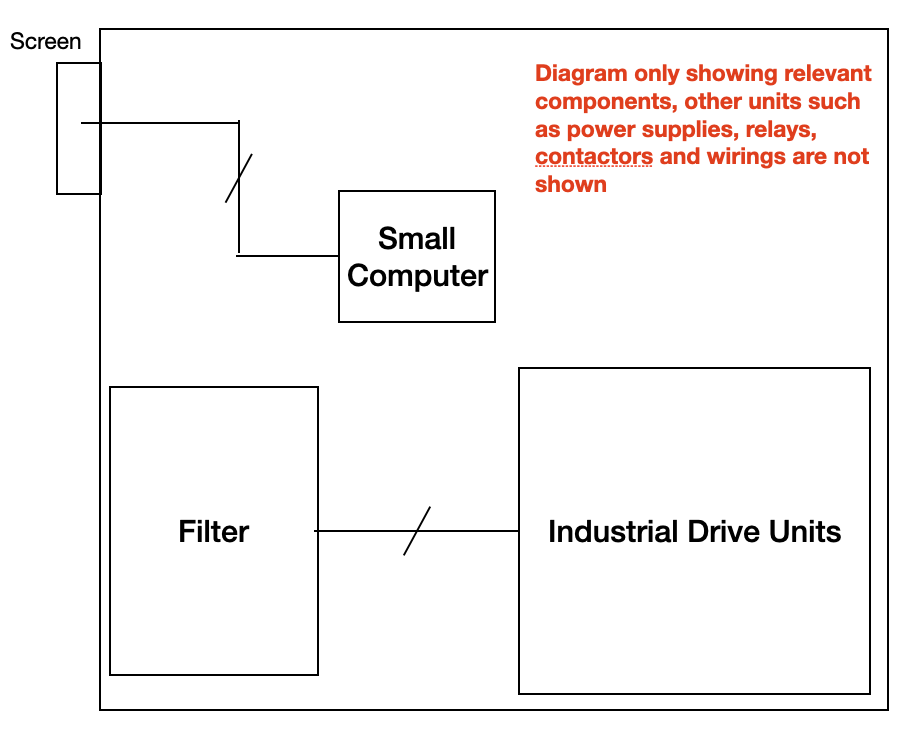
A simplified system diagram is shown below. The unit is a three-phase bi-directional power electronics system. From the initial review, we believed the noise was generated internally rather than from external sources.
The intermittent nature of the problem made troubleshooting particularly challenging. The investigation approach is outlined below.
As with any troubleshooting process, the first step is to reproduce the failure mode before identifying the noise path and implementing solutions. To trigger the screen blackout, a noise source was introduced near the small computer module to replicate the issue observed in the field.
This was achieved using a Langer E1 set. The Langer SGZ 21 burst generator was used, as it can generate high-level burst pulses with two selectable rise times. The amplitude of the pulse can also be adjusted, allowing control over the level of noise injected into the product under test.
In terms of coupling noise into the system, several methods are available, including magnetic and electric field coupling using the accessories provided in the E1 set. In this case, a near-field probe was used.
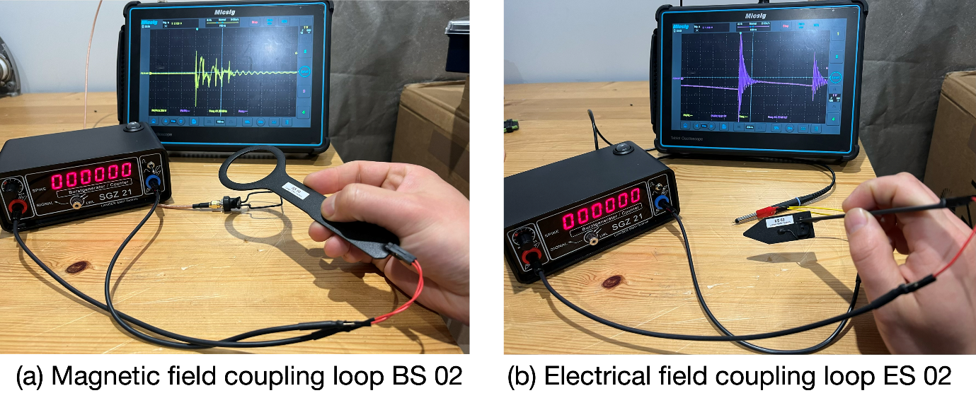
Here, we demonstrate the noise seen by different types of circuits. In the following figure, part (a) shows a small wire loop connected to the 50 Ω input impedance of the oscilloscope. This represents a low-impedance loop circuit commonly found on a PCB, which can readily pick up magnetic fields. When a small level of noise is injected using the BS 02 magnetic field loop probe, a peak-to-peak voltage of approximately 6 V is observed on the oscilloscope—sufficient to disturb a 3.3 V or 5 V circuit.
In part (b), a 10:1 passive probe is connected to the 1 MΩ input impedance of the oscilloscope, representing a high-impedance circuit. When the ES 02 electric field coupling probe is used, the return path of the noise generator is connected to the passive probe’s grounding sleeve. This arrangement allows observation of the noise seen by a high-impedance circuit. With the same low-amplitude setting, peak-to-peak spikes exceeding 10 V were observed.
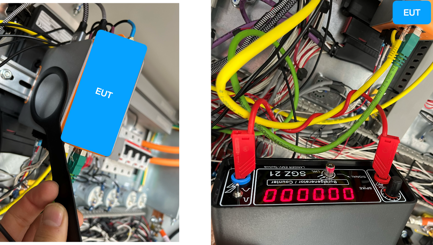
It was observed that when the magnetic field probe BS 02 was positioned at the side of the small computer module, the failure mode could be triggered.
To couple noise into the cables connected to the small computer module, a simple method was used by effectively shorting the output terminals of the noise generator. This forces the generated pulses to flow through a wire. The wire was then wrapped around the cables under test, creating strong magnetic coupling between the generator loop and the cables.
This approach allowed individual cables to be tested one by one to identify those most susceptible to noise.
It was found that the power leads are robust, whereas the Ethernet cables represent the weakest points. This aligns with our experience in similar systems.
So far, the approach has focused on susceptibility. However, the key question remains: why is the small computer module particularly sensitive to noise within the system? To answer this, it is necessary to understand the noise coupling path in order to develop an effective solution.
We then used our emissions troubleshooting kit. In this case, a Langer LF1 set was selected. This set is specifically designed for low-frequency noise pickup and is highly sensitive. Power electronics systems such as this typically exhibit noise from a few kHz up to tens of MHz, with contactor or relay switching introducing transient events, making this probe set well suited to the application.
In addition, as this is a high-voltage system, probing must be carried out at a safe distance. The high sensitivity of the probe therefore becomes particularly important, allowing effective measurements to be made at a safe distance.
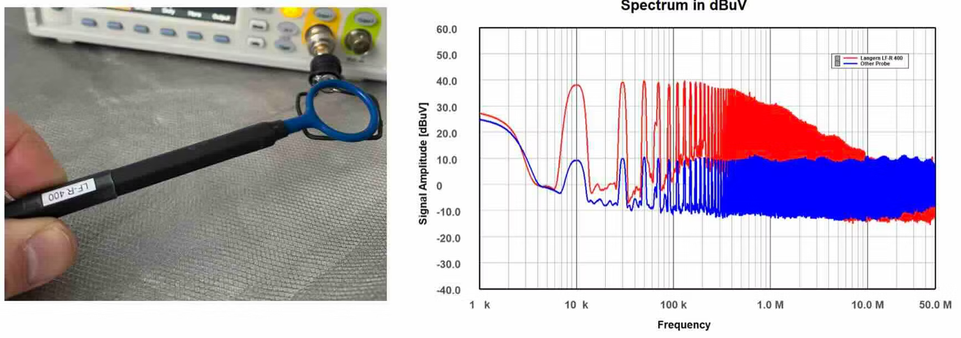
As shown below, the LF-R 400 probe was taped to a safety-insulated rescue stick, allowing safe probing of the areas of interest. The results are convincing: the area where the small computer module is located is very noisy. Measurements were taken in continuous mode, and transient noise was also observed during start-up and shut-down.
Proposed Actions
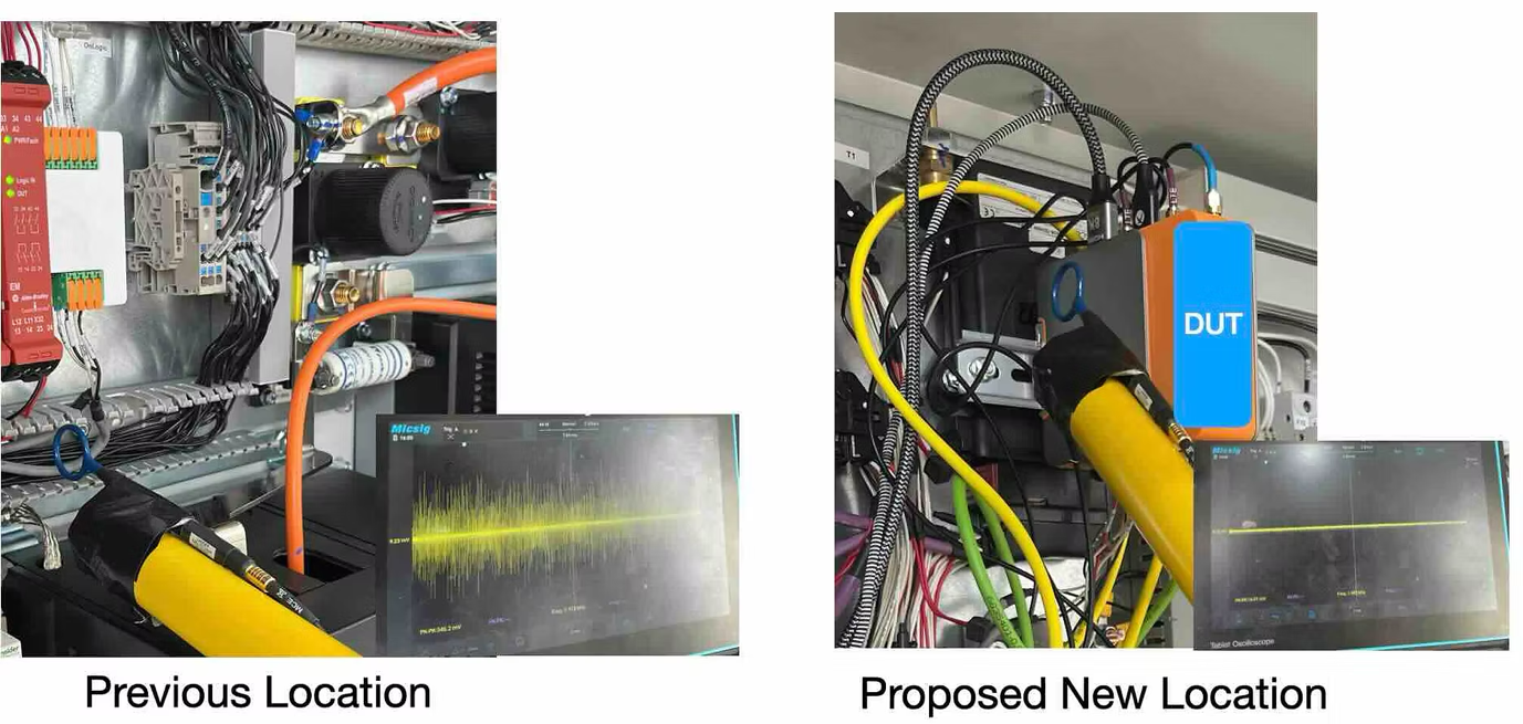
Based on the findings from both the susceptibility testing and emissions mapping within the system, we propose the following actions:
- Relocate the small computer module to a quieter zone within the cabinet. The proposed location has been verified through measurement to exhibit relatively low noise levels.
- Add a ferrite core (material 31) to the Ethernet cable to improve the noise immunity of the module.
Conclusion
By using appropriate test equipment and applying practical field experience, we were able to identify the noise coupling mechanisms and implement effective mitigation measures to improve system robustness.
This approach demonstrates that, even for intermittent EMI issues, a structured troubleshooting method combined with targeted measurements can lead to clear root-cause identification and practical design improvements.
Review of EMV Cologne 2026
EMV Cologne 2026 once again proved to be an excellent platform for us and the central European EMC meeting point for intensive professional exchange and concrete technical discussions drawn directly from practice. The focus of our trade fair appearance was direct dialogue with our customers, developers, and design engineers. At our live consulting area, we analyzed real EMC problems together and addressed practical solution approaches. We complemented this with demonstrations of our development-supporting measurement equipment on specific test objects and demo boards, making typical interference phenomena and their targeted influence during the development process tangible.
A special focus was placed on our new E2 set TS 23 Immunity Development System, which can be used to deliberately generate reproducible disturbance scenarios for fault analysis and design optimization. In addition, we presented the extended capability for the proven near-field probes from Langer EMV-Technik GmbH: RF injection. Once again, the many discussions clearly showed how great the need is for early, practice-oriented EMC analyses. This is exactly where our solutions such as EMC experimental seminars, development-supporting EMC consulting, and our portfolio of EMC tools come in.
The video provides impressions of our trade fair appearance and shows our booth, the technical setups, and selected on-site demonstrations. We would like to thank all visitors for the open exchange and the many technically valuable discussions.